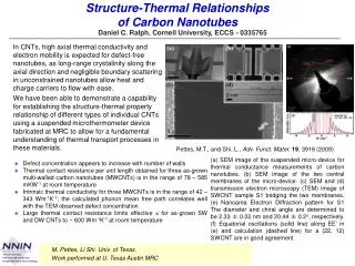
Download
1 / 42
420 likes | 607 Views
Probing the Electronic Structure of Carbon Nanotubes using Rayleigh Scattering. Matthew Y. Sfeir. Feng Wang Limin Huang X. M. H. Huang Mingyuan Huang Jim Hone Stephen O’Brien Tony Heinz Louis Brus. Tobias Beetz Lijun Wu Yimei Zhu Jim Misewich. Imagining the Carbon Nanotube Structure.

E N D
Probing the Electronic Structure of Carbon Nanotubes using Rayleigh Scattering Matthew Y. Sfeir Feng Wang Limin Huang X. M. H. Huang Mingyuan Huang Jim Hone Stephen O’Brien Tony Heinz Louis Brus Tobias Beetz Lijun Wu Yimei Zhu Jim Misewich
Imagining the Carbon Nanotube Structure Family of closely related molecules with hundreds of members and diameters ranging from 0.4 - 3.0 nm. Each nanotube is uniquely described by its diameter [dt] and chiral angle q. [Also can be labeled by (n,m)]
M22 1 S44 S33 M11 S22 S11 Motivation and Open Questions Our understanding of SWNTs mainly comes from: Kataura Plot • Single-particle theory. (LEFT) • Assignments of luminescence data (Box 1) based on predictions from single-particle theory. • Measurement and calcs. confirming the existence of many-body effects. All allowed nanotube transitions (eV) SWNT diameter What is the real electronic structure of an arbitrary SWNT?
1s 2p Band edge Experimental Detemination of Excitons in SWNTs Two photon excitation spectra of individual fluorescence peaks Energy levels of transitions observed directly from 2-photon excitation and emission spectra The optical transitions in nanotubes are excitons, NOT interband transitions. F. Wang et al, Science 308, 838(2005)
Motivation and Open Questions • 1. Assign the optical spectra of all SWNTs. • As there is no accurate theory to guide optical assignments this requires independent measurement of electronic and physical structure. • 2. From assignments, develop understanding of the influence of many-body and chirality effects in both metals and semiconductors. Theory Experiment ?
Optical Methods to Probe SWNTs O'Connell, et al. Science297, 593-596 (2002). 1) Absorption Small cross section, has only previously been measured in ensemble samples. 2) Luminescence Only applicable to small diameter semiconducting tubes. 3) Resonance Raman Scattering Need to satisfy unknown resonance condition; very weak. Raman 4) Rayleigh Scattering Can probe all frequencies simultaneously with white light; can we observe resonant enhancement? cm-1
Linear Light Scattering Processes Resonance Rayleigh Scattering • Elastic light scattering [white light scattering] • wscattered= wincident • Probe electronic structure – detectable at all w, but enhanced at electronic transition energies similar to absorption spectra w Resonance Raman Scattering • Inelastic light scattering – momentum transfer via fundamental excitations in material (monochromatic) • Vibrational Raman – probe Raman active phonons • wscattered = wincident wphonon • Strongly enhanced at energies in resonance with an electronic transition Resonance Raman cm-1 shift from w
Rayleigh Scattering From Nanostructures Resonance Rayleigh scattering shown to closely resemble the absorption spectra. Silver Particles SWNT Bundles Michaels, Amy M.; Nirmal, M.; Brus, L. E. JACS121(43): 9932-9939. (1999) Yu, Z. and Brus, L. J. Phys. Chem. B 105(6): 1123-1134. (2001)
Supercontinuum Radiation for Spectroscopy Smaller cross-section of carbon nanotubes demands a brighter light source compatible with confocal microscopy methods. Solution: white-light generation in an optical fiber: laser brightness with a large spectral bandwidth (450- 1450 nm) log Intensity
10 m Isolated SWNT slit edges nanotube scattering Sample Fabrication and Characterization Growing Suspended Nanotubes Imaging Look at total integrated intensity on CCD to find tubes. Correlate to electron microscopy images. Substrates with slits patterned by optical lithography and wet etching. CVD directional growth with lengths > 100 microns:
Resonance Rayleigh Scattering Spectra M. Sfeir et al, Science 306, 1540 (2004) Semiconducting Carbon Nanotube Two well separated S33 and S44 transitions for larger diameter tubes, S33 and S22 for smaller diameters. Metallic Carbon Nanotube Single M11 or M22 transition observed in the visible – sometimes split into two very close peaks by trigonal warping effect
Theoretical Rayleigh Scattering from a SWNT Treat SWNT as an infinite right cylinder with effective dielectric function. e = e1 + ie2 Band Model Exciton Model Energy Energy Peaks in the dielectric function give rise to peaks in the Rayleigh spectrum; resulting lineshape is similar for exciton or interband model.
TEM Collaboration with the electron microscopy group @ Brookhaven National Labs. Image Diffraction Assigning the Optical Spectra For unambiguous assignment of optical transitions, we need a technique compatible with our sample geometry that provides an independent structural verification.
Equatorial Oscillation Determining SWNT Structure by Electron Diffraction Analyze electron scattering signal from ~ 20 nm collimated electron beam. Gao, et. al., Appl. Phys. Let., 82(16) 2703. (2003)
Intensity a: experimental diffraction b: simulated diffraction Energy (eV) Direct Correlation of the Electronic and Physical Structure M. Sfeir et al, Science accepted (2006) (16, 11) • Optical Transitions: • S33 = 2.0 eV • S44 = 2.3 eV Diameter: 1.83 nm Chiral Angle: 23.9 o
S33 S44 Transition Energies (eV) Rayleigh Spectrum Resonance Energy Fit -Tight Binding Calcs Extended Tight Binding ETB + Many-body Corr. 1.99 2.27 2.00 2.30 1.79 2.14 1.63 1.93 1.88 2.15 (16,11) Electronic Structure Comparisons to some commonly used theoretical treatments. Substantial differences in the absolute energies from theory: Semis: > 200 meV Metals: > 150 meV
Testing Fundamental Predictions of Electronic Structure A predicted chirality dependence leads to systematic deviations as a function of (n,m). Do many-body effects (which shift absolute energies) disrupt this pattern? Zoom of region of Kataura plot Ignoring chirality and many-body effects: S33 M11 However, the graphene energy dispersion is not a linear function of k.
Testing Fundamental Predictions of Electronic Structure A predicted chirality dependence leads to systematic deviations as a function of (n,m). Do many-body effects (which shift absolute energies) disrupt this pattern? Zoom of region of Kataura plot Spread within a transition series is not random and depends on chirality [(n,m)]. S33 2n+m=46 Semiconducting: “family” behavior 2n+m=44 • Within certain structural "families" (changing d and q), energies evolve in a predictable way within that group. M11 Metals: trigonal warping effect • Splitting of transitions within a series with increasing chiral angle It is difficult to measure these effects experimentally because of little correlation between optical and physical data!
Semiconducting SWNTS 1. Constant Chiral Angle 2. Constant Diameter D dt = 0.12 nm D q = 5.3o We can use these three patterns to indirectly assign many of our spectra! 3. Families of Constant 2n+m Our data confirms some “family” behavior – the relationships between SWNTs with different diameters and chiral angles.
Metallic SWNTs Experimental Verification of the Trigonal Warping Effect Not detectable by luminescence of Raman scattering - shows unique capabilities of the Rayleigh scattering method. M22 M11 M11 q = 24o q = 30o q = 25o DE = 90 meV DE = 140 meV DE = 0 meV
M22 S44 S33 M11 S22 S11 Connecting Different Data Sets How do we compare nanotubes from different regions of the Kataura plot to develop a universal picture of excited states? We have optical data for: Small diameter semi SWNTs. [diameters < 1 nm] Strong many-body effects Large diameter semi SWNTs [diameters > 1.6 nm] Unknown many-body effects? Metallic nanotubes with diameters in between [1.3 nm] No many body-effects??? 2 3 1
2.00 S33 M11 1.95 (14,13) S22 (10,10) (7,6) 1.7nm 1.3 nm 0.8 nm 1.90 1.85 2.10 2.15 2.20 2.25 2.30 Connecting Different Data Sets Kane CL, Mele EJ. PRL 93 197402 (2004). Nanotube electronic structure dominated by 2D many-body effects (REAL graphene dispersion). 1D are negligible. We don’t know the real graphene energy dispersion: E(k) For SWNT transitions with energy E, determine k, and compare different nanotubes with similar k. If 1D effects are strong, this treatment will give large errors (metal vs. semi; diameter dependence). k This is the best theoretical fit to our data and implies that metals and semiconductors not very different!!!
Synthesis and Fabrication O’Brien, Hone Transfer Technology Intertube Interactions Hone Heinz, Brus Hone, Kim Mechanical Transport Heinz, Hone NSEC Electro-optics Theory Heinz, Brus Heinz, Hone, BNL Raman Scattering SWNT Project Synergy Many projects have contributed to and benefitted from the Rayleigh scattering project and furthered our understanding of SWNTs.
Conclusions We have developed an optical method useful for identifying the optically allowed electronic transitions in individual carbon nanotubes. Rayleigh scattering spectra can be interpreted qualitatively using theory as a guide but direct structual characterization is necessary for assignments. We have begun building a set of assignments from correlated electron diffraction measurements and extending those using the expected evolution . An interesting picture of the excited states is emerging – we invite theoretical help with this problem!!!
Acknowledgements Optical Experiments: Feng Wang Yang Wu Tony Heinz Louis Brus Production and Growth: Jim Hone Limin Huang Henry Huang Mingyuan Huang Discussion: Mark Hybertsen Philip Kim Gordana Dukovic Jim Yardley Jim Misewich, BNL Electron Microscopy: Limin Huang Lijun Wu, BNL Yimei Zhu, BNL Tobias Beetz, BNL
37 41 47 44 37 40 43 40 Eii (eV) 46 38 43 41 44 47 1/dt Examining “Family” Relations We have seen that our data progresses in the expected way for diameter and chirality changes.
Chirality Dependence in a Non-interacting Model Metal Semiconductor - I Semiconductor - II mod (n – m, 3) = 1 mod (n – m, 3) = 2 mod (n – m, 3) = 0 Metals: “trigonal warping effect” Semiconductors: “family” behavior
Trigonal Warping Effect in Metallic SWNT Constant energy contours of graphene dispersion = 30o Saito et. al., PRB 61, 2981 (2000). Reich and Thomsen, PRB 62, 4273 (2000). = 0o
Can we extend this technique to a single nanotube? The nanotube has an extremely small scattering cross-section. Silver (50 nm) SWNT (40 m long) N2 10-27 cm2 10-14 cm2 10-10 cm2 Need a sufficiently bright broadband excitation source and a single nanotube in a controlled geometry and environment.
dt = 1.89 nm eV Resonantly excite at ONE energy (1.96 eV) Structural Information from Raman Scattering Rayleigh Identifies MULTIPLE electronic transitions which can be used to satisfy the resonance condition needed for Raman. Resonance Raman: (21,4) nanotube? Low chiral angle Phonon frequency (cm-1)
Using Rayleigh Information To Engineer Nanotube Devices Henry’s Transfer Method X. M. H. Huang, R. Caldwell, L. Huang, S. Jun, M. Huang, M.Y. Sfeir, L. Brus, S.P. O’Brien, J. Hone, Submitted, 2005. This gives us the ability to select a nanotube with specific properties and place it on a surface with spatial accuracy of several microns.
An Example with Electronic Transport Data 1. Optical Characterization: • Semiconducting Nanotube • dt ~ 1.9 nm • (17,10) possible assignment from family plots 2. Transfer to Si substrate for transport measurements: • Confirms semiconducting character
B A Scattering Spectra along the Nanotube: Single Tube to Small Bundle B A Semiconducting Metallic Transitions red-shift by 20 - 50 meV upon bundling.
A A A+B A+B B B Nanotube Bundling in a Y-Junction A: Moderate sized bundle structure. B: Single semiconducting nanotube with dt ~ 1.9 nm. A+B: Merged structure. The resonances in tube B are red-shifted by 35 and 47 meV. The resonances in tube A are shifted by much less in the combined structure. This effect is consistent with dielectric screening of manybody effects.
Polarization Dependence of Rayleigh Scattering X 5 Polarization along nanotube axis: Selection rules allow symmetric transitions between singularities in the DOS, J = 0. Perpendicular to nanotube axis: Selection rules allow J =1 transitions, but quenched due to “depolarization effect.”
eV Lineshape Analysis Rayleigh Scattering Exciton Model Band Model
Dielectric Function Optical response is dominated by the peaked joint density of states. We observe Rayleigh scattering that is resonantly enhanced near the absorption maxima.
Rayleigh Spectra Collected with a QTH Lamp Collection time > 4.5 hours per graph.
eV Lineshape Analysis Rayleigh Scattering Exciton Model Band Model