Download
1 / 20
200 likes | 309 Views
TEAM LLAMP. Nadja Memic Steve Karcher Sri Teja Basava Francis Yi. Laser Lattice Associative Multi-touch Product Preliminary Design Review. PDR Outline. Project Objectives Outline of Approach Frame Input Processing Box Driver Implementation of Subsystems Division of Labor Timeline

E N D
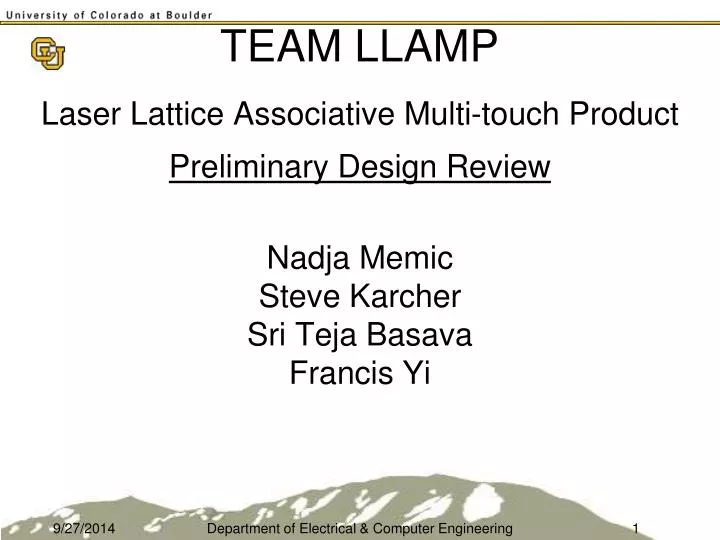
TEAM LLAMP Nadja Memic Steve Karcher Sri Teja Basava Francis Yi Laser Lattice Associative Multi-touch Product Preliminary Design Review Department of Electrical & Computer Engineering
PDR Outline • Project Objectives • Outline of Approach • Frame • Input Processing Box • Driver • Implementation of Subsystems • Division of Labor • Timeline • Build or Buy? • Costs • Risks • Questions? Department of Electrical & Computer Engineering
Project Objectives Department of Electrical & Computer Engineering
Project Objectives 40” User Input Area Multi-touch Support Simple Drawing Tool Extensions Multi-user Software Application e.g. Classroom Finder, Public Information Kiosk Department of Electrical & Computer Engineering
Outline of Approach Touch Input FPGA Rx Status Frame Input Processing Box N USB 2.0 Interrupted X and Y Positions Computer Driver Software Application (Drawing Tool) Pointer Coordinates N Number of sensors Screen Output Department of Electrical & Computer Engineering
Frame Functionality Gets multi-touch input from user Inputs User input Outputs Signals indicating Rx status Department of Electrical & Computer Engineering
Frame … Nx Tx Tx VT + 40” Input Area - Tx Rx Analog Tx Rx Analog - … … + VT … Ny Ny VT + Rx Rx Nx - Analog Analog - Nx Number of horizontal Rx/Tx Ny Number of vertical Rx/Tx VT Threshold Voltage + VT Department of Electrical & Computer Engineering
Input Processing Box Functionality Processes and converts the interrupts for use by the driver Inputs Signals indicating Rx status Outputs Data indicating interrupted x and y positions Department of Electrical & Computer Engineering
Input Processing Box Clock Change Logic Memory Buffer USB Interface Parallel to Serial Conversion Logic Clock Department of Electrical & Computer Engineering
Driver Functionality Gets the contents of memory buffer and interprets the x and y position data. This can then be used by the computer to control a mouse pointer. Inputs Data indicating interrupted x and y positions from memory buffer Outputs Mouse control signal Department of Electrical & Computer Engineering
Driver USB Driver Proximity Detection Module Average Calculation Module Department of Electrical & Computer Engineering
Implementation of Subsystems Pictures from left to right from: http://www.knjn.com/ShopItemsPics/Board_Xylo-L.jpg, http://en.wikipedia.org/wiki/Image:Windowsloadingdrivers.jpg, http://www.publicdataweb.com/PDW/images/gif/Kiosk-BusStop-Anime.gif Department of Electrical & Computer Engineering
Division of Labor and Responsibilities • 1.Frame: • - Housing • - Circuitry/Board • - Tx/Rx Research • 2.Input Processing Box: • - FPGA choice • - Logic algorithm development • - Adapting to our platform • 3.Driver Development: • - Updating, averaging, proximity & toggling • Software Application: • - Implementation of painting ftn Francis & Nadja Steve & Teja Entire Team Entire Team Steve & Teja Francis, Nadja & Teja Francis, Steve & Nadja Teja & Francis Department of Electrical & Computer Engineering
User Input Area Test and choose solution Grid construction Choose logic solution Input processing box Develop on DEV board Write driver code Application System Wide Integration Board Layout Develop support circuitry Transplant DEV board Timeline Department of Electrical & Computer Engineering
Timeline Department of Electrical & Computer Engineering
Timeline Department of Electrical & Computer Engineering
Build or Buy Decisions Buy Power Supplies Projector Computer USB Module FPGA Chip Laser Diodes Photodiodes Build Frame Logic Circuit / Board Layout Driver Software Software (Paint, Kiosk) Interconnections between sensors and FPGA Pictures from: http://www.eio.com/repairfaq/sam/ldclose.gif, http://img.engadget.com/common/images/3363705371535783.JPG?0.299055096787738, http://www.futurlec.com.au/images/USBMOD1.jpg, http://static.howstuffworks.com/gif/power-supply5.jpg, http://www.itreviews.co.uk/graphics/normal/hardware/h930.jpg Department of Electrical & Computer Engineering
Costs Department of Electrical & Computer Engineering
Risks and Contingency Plan • Risks: • Dead spots • Differentiating between inputs • Laser alignment within frame • Cost of laser diodes • Health risk • Time to complete • Lack of Experience • Plan B: • Capacitive touch-screen design • Different algorithms or single touch • Manually aligning the lasers • Smaller user area • Resort to LED rather than lasers • Implement a weaker light source • Cut back on software applications Source: http://www.eyemdlink.com/images/illustrations/small/yagLaser.jpg Department of Electrical & Computer Engineering
Questions? ? Thank You! Department of Electrical & Computer Engineering

![[Team name] Team Award](https://cdn4.slideserve.com/678300/slide1-dt.jpg)