Download
1 / 61
620 likes | 623 Views
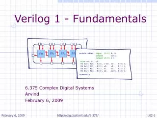
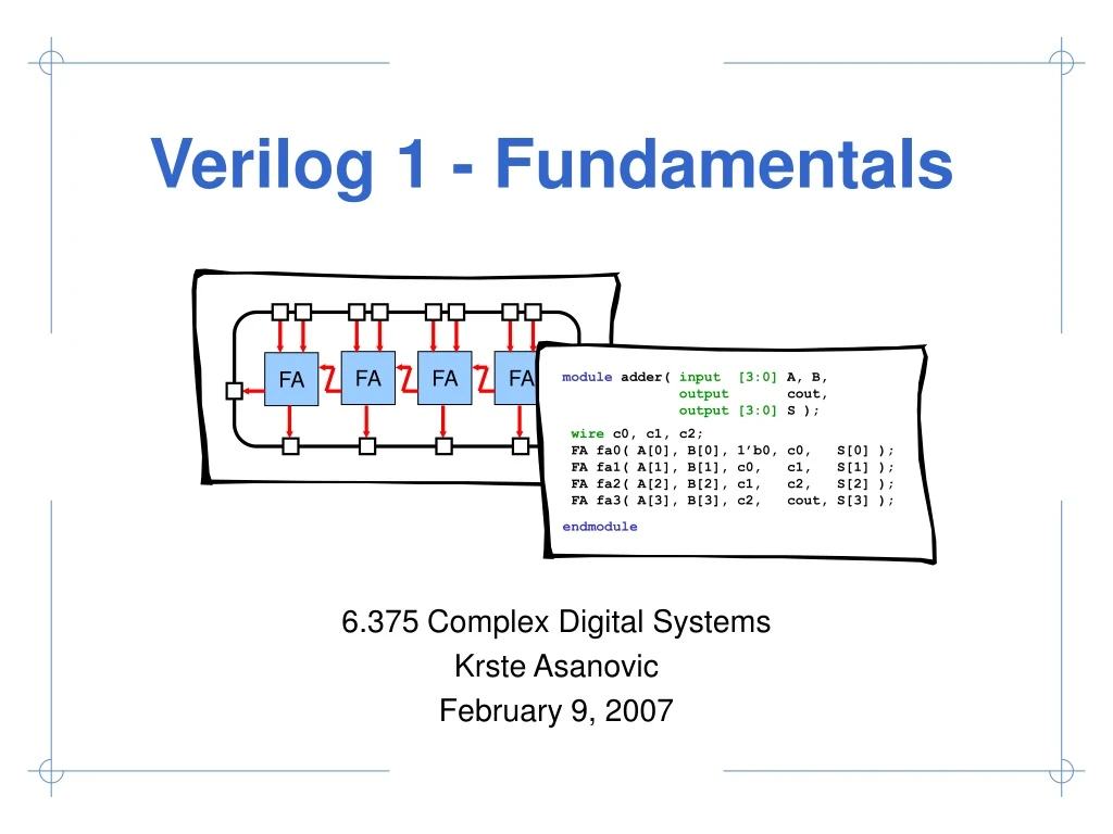
FA. FA. FA. FA. module adder( input [3:0] A, B, output cout, output [3:0] S ); wire c0, c1, c2; FA fa0( A[0], B[0], 1’b0, c0, S[0] ); FA fa1( A[1], B[1], c0, c1, S[1] ); FA fa2( A[2], B[2], c1, c2, S[2] ); FA fa3( A[3], B[3], c2, cout, S[3] ); endmodule.

E N D
FA FA FA FA module adder( input [3:0] A, B, output cout, output [3:0] S ); wire c0, c1, c2; FA fa0( A[0], B[0], 1’b0, c0, S[0] ); FA fa1( A[1], B[1], c0, c1, S[1] ); FA fa2( A[2], B[2], c1, c2, S[2] ); FA fa3( A[3], B[3], c2, cout, S[3] ); endmodule Verilog 1 - Fundamentals 6.375 Complex Digital Systems Krste Asanovic February 9, 2007
FA FA FA FA module adder( input [3:0] A, B, output cout, output [3:0] S ); wire c0, c1, c2; FA fa0( A[0], B[0], 1’b0, c0, S[0] ); FA fa1( A[1], B[1], c0, c1, S[1] ); FA fa2( A[2], B[2], c1, c2, S[2] ); FA fa3( A[3], B[3], c2, cout, S[3] ); endmodule Verilog Fundamentals • History of hardware design languages • Data types • Structural Verilog • Functional Verilog • Gate level • Register transfer level • High-level behavioral
Bread Board Test Results Originally designers used manual translation + bread boards for verification Number of Gates in Design Behavioral Algorithm 107 Manual 106 Register Transfer Level 105 Manual 104 Gate Level 103 Manual 102 10
Simulate Test Results Hardware design languages enabled logic level simulation and verification Number of Gates in Design Behavioral Algorithm 107 Manual 106 Register Transfer Level 105 Manual 104 Gate Level 103 Manual 102 10
Simulate Test Results Simulate Test Results Designers began to use HDLs for higher level verification and design exploration Number of Gates in Design Behavioral Algorithm 107 Manual 106 Register Transfer Level 105 Manual 104 Gate Level 103 Manual 102 10
Simulate Test Results Simulate Test Results Simulate Test Results HDL behavioral models act as a precise and executable specification Number of Gates in Design Behavioral Algorithm 107 Manual 106 Register Transfer Level 105 Manual 104 Gate Level 103 Manual 102 10
Once designs were written in HDLs tools could be used for automatic translation Number of Gates in Design Simulate Behavioral Algorithm Test Results 107 Manual Simulate 106 Test Results Register Transfer Level 105 Manual 104 Simulate Test Results Gate Level 103 Auto Place + Route 102 10
Once designs were written in HDLs tools could be used for automatic translation Number of Gates in Design Simulate Behavioral Algorithm Test Results 107 Manual Simulate 106 Test Results Register Transfer Level 105 Logic Synthesis 104 Simulate Test Results Gate Level 103 Auto Place + Route 102 10
Guarded atomic actions can help us to efficiently raise the abstraction level Number of Gates in Design Simulate Behavioral Algorithm Test Results 107 Manual Simulate 106 Test Results Guarded Atomic Actions 105 Action Compiler 104 Simulate Test Results Register Transfer Level 103 Logic Synthesis 102 Simulate Test Results Gate Level 10
FA FA FA FA module adder( input [3:0] A, B, output cout, output [3:0] S ); wire c0, c1, c2; FA fa0( A[0], B[0], 1’b0, c0, S[0] ); FA fa1( A[1], B[1], c0, c1, S[1] ); FA fa2( A[2], B[2], c1, c2, S[2] ); FA fa3( A[3], B[3], c2, cout, S[3] ); endmodule Verilog Fundamentals • History of hardware design languages • Data types • Structural Verilog • Functional Verilog • Gate level • Register transfer level • High-level behavioral
An X bit might be a 0, 1, Z, or in transition. We can set bits to be X in situations where we don’t care what the value is. This can help catch bugs and improve synthesis quality. Primary Verilog data type is a bit-vector where bits can take on one of four values
? The Verilog keyword wire is used to denote a standard hardware net wire [15:0] instruction; wire [15:0] memory_req; wire [ 7:0] small_net; Absolutely no type safety when connecting nets! small_net instruction memory_req instruction
Verilog includes ways to specify bit literals in various bases • Binary literals • 8’b0000_0000 • 8’b0xx0_1xx1 • Hexadecimal literals • 32’h0a34_def1 • 16’haxxx • Decimal literals • 32’d42 4’b10_11 Underscores are ignored Base format (d,b,o,h) Decimal number representing size in bits We’ll learn how to actually assign literals to nets a little later
FA FA FA FA module adder( input [3:0] A, B, output cout, output [3:0] S ); wire c0, c1, c2; FA fa0( A[0], B[0], 1’b0, c0, S[0] ); FA fa1( A[1], B[1], c0, c1, S[1] ); FA fa2( A[2], B[2], c1, c2, S[2] ); FA fa3( A[3], B[3], c2, cout, S[3] ); endmodule Verilog Basics • History of hardware design languages • Data types • Structural Verilog • Functional Verilog • Gate level • Register transfer level • High-level behavioral
Ports must have a direction (or be bidirectional) and a bitwidth Note the semicolon at the end of the port list! A Verilog module includes a module name and a port list A B module adder( A, B, cout, sum ); input [3:0] A; input [3:0] B; output cout; output [3:0] sum; // HDL modeling of // adder functionality endmodule 4 4 adder 4 cout sum
A Verilog module includes a module name and a port list Traditional Verilog-1995 Syntax module adder( A, B, cout, sum ); input [3:0] A; input [3:0] B; output cout; output [3:0] sum; ANSI C Style Verilog-2001 Syntax module adder( input [3:0] A, input [3:0] B, output cout, output [3:0] sum ); A B 4 4 adder 4 cout sum
A module can instantiate other modules creating a module hierarchy a b module FA( input a, b, cin output cout, sum ); // HDL modeling of 1 bit // full adder functionality endmodule cin FA cout c
A module can instantiate other modules creating a module hierarchy A B FA FA FA FA adder cout S module adder( input [3:0] A, B, output cout, output [3:0] S ); wire c0, c1, c2; FA fa0( ... ); FA fa1( ... ); FA fa2( ... ); FA fa3( ... ); endmodule
Carry Chain A module can instantiate other modules creating a module hierarchy A B FA FA FA FA adder cout S module adder( input [3:0] A, B, output cout, output [3:0] S ); wire c0, c1, c2; FA fa0( A[0], B[0], 1’b0, c0, S[0] ); FA fa1( A[1], B[1], c0, c1, S[1] ); FA fa2( A[2], B[2], c1, c2, S[2] ); FA fa3( A[3], B[3], c2, cout, S[3] ); endmodule
Verilog supports connecting ports by position and by name Connecting ports by ordered list FA fa0( A[0], B[0], 1’b0, c0, S[0] ); Connecting ports by name (compact) FA fa0( .a(A[0]), .b(B[0]), .cin(1’b0), .cout(c0), .sum(S[0]) ); Connecting ports by name FA fa0 ( .a (A[0]), .b (B[0]), .cin (1’b0), .cout (c0), .sum (S[0]) ); For all but the smallest modules, connecting ports by name yields clearer and less buggy code.
Let’s review how to turn our schematic diagram into structural Verilog FA FA FA FA
FA FA FA FA module adder( input [3:0] A, B, output cout, output [3:0] S ); endmodule module adder( input [3:0] A, B, output cout, output [3:0] S ); FA fa0( ... ); FA fa1( ... ); FA fa2( ... ); FA fa3( ... ); endmodule module adder( input [3:0] A, B, output cout, output [3:0] S ); wire c0, c1, c2; FA fa0( A[0], B[0], 1’b0, c0, S[0] ); FA fa1( A[1], B[1], c0, c1, S[1] ); FA fa2( A[2], B[2], c1, c2, S[2] ); FA fa3( A[3], B[3], c2, cout, S[3] ); endmodule Let’s review how to turn our schematic diagram into structural Verilog module adder( ... ); endmodule
FA FA FA FA module adder( input [3:0] A, B, output cout, output [3:0] S ); wire c0, c1, c2; FA fa0( A[0], B[0], 1’b0, c0, S[0] ); FA fa1( A[1], B[1], c0, c1, S[1] ); FA fa2( A[2], B[2], c1, c2, S[2] ); FA fa3( A[3], B[3], c2, cout, S[3] ); endmodule Verilog Fundamentals • History of hardware design languages • Data types • Structural Verilog • Functional Verilog • Gate level • Register transfer level • High-level behavioral
Functional Verilog can roughly be divided into three abstraction levels Behavioral Algorithm V Abstract algorithmic description Manual Describes how data flows between state elements for each cycle Register Transfer Level V Logic Synthesis Low-level netlist of primitive gates V Gate Level Auto Place + Route
Gate-level Verilog uses structural Verilog to connect primitive gates module mux4( input a, b, c, d, input [1:0] sel, output out ); wire [1:0] sel_b; not not0( sel_b[0], sel[0] ); not not1( sel_b[1], sel[1] ); wire n0, n1, n2, n3; and and0( n0, c, sel[1] ); and and1( n1, a, sel_b[1] ); and and2( n2, d, sel[1] ); and and3( n3, b, sel_b[1] ); wire x0, x1; nor nor0( x0, n0, n1 ); nor nor1( x1, n2, n3 ); wire y0, y1; or or0( y0, x0, sel[0] ); or or1( y1, x1, sel_b[0] ); nand nand0( out, y0, y1 ); endmodule sel[0] b d a c sel[1] out
Continuous assignment statements assign one net to another or to a literal Explicit continuous assignment wire [15:0] netA; wire [15:0] netB; assign netA = 16’h3333; assign netB = netA; Implicit continuous assignment wire [15:0] netA = 16’h3333; wire [15:0] netB = netA;
Using continuous assignments to implement an RTL four input multiplexer module mux4( input a, b, c, d input [1:0] sel, output out ); wire out, t0, t1; assign out = ~( (t0 | sel[0]) & (t1 | ~sel[0]) ); assign t1 = ~( (sel[1] & d) | (~sel[1] & b) ); assign t0 = ~( (sel[1] & c) | (~sel[1] & a) ); endmodule module mux4( input a, b, c, d input [1:0] sel, output out ); wire out, t0, t1; assign t0 = ~( (sel[1] & c) | (~sel[1] & a) ); assign t1 = ~( (sel[1] & d) | (~sel[1] & b) ); assign out = ~( (t0 | sel[0]) & (t1 | ~sel[0]) ); endmodule The order of these continuous assignment statements does not matter. They essentially happen in parallel!
If input is undefined we want to propagate that information. Verilog RTL includes many operators in addition to basic boolean logic // Four input multiplexer module mux4( input a, b, c, d input [1:0] sel, output out ); assign out = ( sel == 0 ) ? a : ( sel == 1 ) ? b : ( sel == 2 ) ? c : ( sel == 3 ) ? d : 1’bx; endmodule // Simple four bit adder module adder( input [3:0] op1, op2, output [3:0] sum ); assign sum = op1 + op2; endmodule
Verilog RTL operators wire [ 3:0] net1 = 4’b00xx; wire [ 3:0] net2 = 4’b1110; wire [11:0] net3 = { 4’b0, net1, net2 }; wire equal = ( net3 === 12’b0000_1110_00xx ); Avoid ( / % ** ) since they usually synthesize poorly
Always blocks have parallel inter-block and sequential intra-block semantics module mux4( input a, b, c, d input [1:0] sel, output out ); reg out, t0, t1; always@( a or b or c or d or sel ) begin t0 = ~( (sel[1] & c) | (~sel[1] & a) ); t1 = ~( (sel[1] & d) | (~sel[1] & b) ); out = ~( (t0 | sel[0]) & (t1 | ~sel[0]) ); end endmodule The always block is reevaluated whenever a signal in its sensitivity list changes
Always blocks have parallel inter-block and sequential intra-block semantics module mux4( input a, b, c, d input [1:0] sel, output out ); reg out, t0, t1; always@( a or b or c or d or sel ) begin t0 = ~( (sel[1] & c) | (~sel[1] & a) ); t1 = ~( (sel[1] & d) | (~sel[1] & b) ); out = ~( (t0 | sel[0]) & (t1 | ~sel[0]) ); end endmodule The order of these procedural assignment statements does matter. They essentially happen sequentially!
Always blocks have parallel inter-block and sequential intra-block semantics module mux4( input a, b, c, d input [1:0] sel, output out ); reg out, t0, t1; always@( a or b or c or d or sel ) begin t0 = ~( (sel[1] & c) | (~sel[1] & a) ); t1 = ~( (sel[1] & d) | (~sel[1] & b) ); out = ~( (t0 | sel[0]) & (t1 | ~sel[0]) ); end endmodule LHS of procedural assignments must be declared as a reg type. Verilog reg is not necessarily a hardware register!
Always blocks have parallel inter-block and sequential intra-block semantics module mux4( input a, b, c, d input [1:0] sel, output out ); reg out, t0, t1; always@( a or b or c or d or sel ) begin t0 = ~( (sel[1] & c) | (~sel[1] & a) ); t1 = ~( (sel[1] & d) | (~sel[1] & b) ); out = ~( (t0 | sel[0]) & (t1 | ~sel[0]) ); end endmodule What happens if we accidentally forget a signal on the sensitivity list?
Always blocks have parallel inter-block and sequential intra-block semantics module mux4( input a, b, c, d input [1:0] sel, output out ); reg out, t0, t1; always@( * ) begin t0 = ~( (sel[1] & c) | (~sel[1] & a) ); t1 = ~( (sel[1] & d) | (~sel[1] & b) ); out = ~( (t0 | sel[0]) & (t1 | ~sel[0]) ); end endmodule Verilog-2001 provides special syntax to automatically create a sensitivity list for all signals read in the always block
Continuous and procedural assignment statements are very different Continuous assignments are for naming and thus we cannot have multiple assignments for the same wire wire out, t0, t1; assign t0 = ~( (sel[1] & c) | (~sel[1] & a) ); assign t1 = ~( (sel[1] & d) | (~sel[1] & b) ); assign out = ~( (t0 | sel[0]) & (t1 | ~sel[0]) ); Procedural assignments hold a value semantically, but it is important to distinguish this from hardware state reg out, t0, t1, temp; always@( * ) begin temp = ~( (sel[1] & c) | (~sel[1] & a) ); t0 = temp; temp = ~( (sel[1] & d) | (~sel[1] & b) ); t1 = temp; out = ~( (t0 | sel[0]) & (t1 | ~sel[0]) ); end
Always blocks can contain more advanced control constructs module mux4( input a, b, c, d input [1:0] sel, output out ); reg out; always@( * ) begin case ( sel ) 2’d0 : out = a; 2’d1 : out = b; 2’d2 : out = c; 2’d3 : out = d; default : out = 1’bx; endcase end endmodule module mux4( input a, b, c, d input [1:0] sel, output out ); reg out; always@( * ) begin if ( sel == 2’d0 ) out = a; elseif ( sel == 2’d1 ) out = b elseif ( sel == 2’d2 ) out = c elseif ( sel == 2’d3 ) out = d else out = 1’bx; end endmodule
What happens if the case statement is not complete? module mux3( input a, b, c input [1:0] sel, output out ); reg out; always@( * ) begin case ( sel ) 2’d0 : out = a; 2’d1 : out = b; 2’d2 : out = c; endcase end endmodule If sel = 3, mux will output the previous value. What have we created?
What happens if the case statement is not complete? module mux3( input a, b, c input [1:0] sel, output out ); reg out; always@( * ) begin case ( sel ) 2’d0 : out = a; 2’d1 : out = b; 2’d2 : out = c; default : out = 1’bx; endcase end endmodule We can prevent creating state with a default statement
module flipflop ( input clk, input d, output q ); always @( posedge clk ) begin q = d; end endmodule Edge-triggered always block So is this how we make latches and flip-flops? module latch ( input clk, input d, outputreg q ); always @( clk ) begin if ( clk ) q = d; end endmodule
To understand why we need to know more about Verilog execution semantics wire A_in, B_in, C_in; reg A_out, B_out, C_out; always @( posedge clk ) A_out = A_in; assign B_in = A_out + 1; always @( posedge clk ) B_out = B_in; assign C_in = B_out + 1; always @( posedge clk ) C_out = C_in; A B C +1 +1
To understand why we need to know more about Verilog execution semantics wire A_in, B_in, C_in; reg A_out, B_out, C_out; always @( posedge clk ) A_out = A_in; assign B_in = A_out + 1; always @( posedge clk ) B_out = B_in; assign C_in = B_out + 1; always @( posedge clk ) C_out = C_in; Active Event Queue A 1 On clock edge all those events which are sensitive to the clock are added to the active event queue in any order! B 2 C
A To understand why we need to know more about Verilog execution semantics wire A_in, B_in, C_in; reg A_out, B_out, C_out; always @( posedge clk ) A_out = A_in; assign B_in = A_out + 1; always @( posedge clk ) B_out = B_in; assign C_in = B_out + 1; always @( posedge clk ) C_out = C_in; Active Event Queue A 1 B 2 C
A B To understand why we need to know more about Verilog execution semantics wire A_in, B_in, C_in; reg A_out, B_out, C_out; always @( posedge clk ) A_out = A_in; assign B_in = A_out + 1; always @( posedge clk ) B_out = B_in; assign C_in = B_out + 1; always @( posedge clk ) C_out = C_in; Active Event Queue A 1 B 2 C
A B C To understand why we need to know more about Verilog execution semantics wire A_in, B_in, C_in; reg A_out, B_out, C_out; always @( posedge clk ) A_out = A_in; assign B_in = A_out + 1; always @( posedge clk ) B_out = B_in; assign C_in = B_out + 1; always @( posedge clk ) C_out = C_in; Active Event Queue A 1 B 2 C
A B C B C 1 To understand why we need to know more about Verilog execution semantics wire A_in, B_in, C_in; reg A_out, B_out, C_out; always @( posedge clk ) A_out = A_in; assign B_in = A_out + 1; always @( posedge clk ) B_out = B_in; assign C_in = B_out + 1; always @( posedge clk ) C_out = C_in; Active Event Queue A 1 A evaluates, A_out changes, and as a consequence 1 is added to the event queue B 2 C
B C 1 1 2 C To understand why we need to know more about Verilog execution semantics wire A_in, B_in, C_in; reg A_out, B_out, C_out; always @( posedge clk ) A_out = A_in; assign B_in = A_out + 1; always @( posedge clk ) B_out = B_in; assign C_in = B_out + 1; always @( posedge clk ) C_out = C_in; Active Event Queue A 1 B evaluates, using new value of A_out, and as a consequence 2 is added to the event queue B 2 C Race Condition!
B C 1 1 2 C To understand why we need to know more about Verilog execution semantics wire A_in, B_in, C_in; reg A_out, B_out, C_out; always @( posedge clk ) A_out = A_in; assign B_in = A_out + 1; always @( posedge clk ) B_out = B_in; assign C_in = B_out + 1; always @( posedge clk ) C_out = C_in; Active Event Queue A 1 Event queue is emptied before we go to next clock cycle B 2 C
To understand why we need to know more about Verilog execution semantics wire A_in, B_in, C_in; reg A_out, B_out, C_out; always @( posedge clk ) A_out = A_in; assign B_in = A_out + 1; always @( posedge clk ) B_out = B_in; assign C_in = B_out + 1; always @( posedge clk ) C_out = C_in; Active Event Queue A 1 Event queue is emptied before we go to next clock cycle B 2 C
We didn’t model what we expected due to Verilog execution semantics wire A_in, B_in, C_in; reg A_out, B_out, C_out; always @( posedge clk ) A_out = A_in; assign B_in = A_out + 1; always @( posedge clk ) B_out = B_in; assign C_in = B_out + 1; always @( posedge clk ) C_out = C_in; A B C +1 +1 A 1 B +1 +1 2 C