Download
1 / 15
150 likes | 278 Views
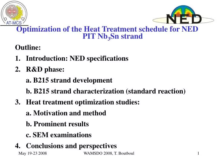
Optimization of the Heat Treatment schedule for NED PIT Nb 3 Sn strand Outline: Introduction: NED specifications R&D phase: a. B215 strand development b. B215 strand characterization (standard reaction) 3. Heat treatment optimization studies: a. Motivation and method

E N D
Optimization of the Heat Treatment schedule for NED PIT Nb3Sn strand • Outline: • Introduction: NED specifications • R&D phase: • a. B215 strand development • b. B215 strand characterization (standard reaction) • 3. Heat treatment optimization studies: • a. Motivation and method • b. Prominent results • c. SEM examinations • 4. Conclusions and perspectives WAMSDO 2008, T. Boutboul
Introduction: NED specifications • NED main goal- to design and build Nb3Sn high-field magnet but mainly limited to conductor due to financial constraints. • Main specifications for NED strand • Diameter 1.250 mm, • Eff. filament diameter < 50 µm, • Cu-to-non-Cu ratio 1.25 ± 0.10, • Filament twist pitch 30 mm, • non-Cu JC (target)1500 A/mm2 @4.2 K & 15 T, • minimum critical current 1636 A at 12 T, • (target)818 A at 15 T, • RRR (after heat treatment) > 200. • Two orders were placed in 2004 to Alstom-MSA (IT) and SMI (PIT) WAMSDO 2008, T. Boutboul
R&D phase: B215 strand development • During R&D phase, SMI developed successfully a strand, B215, including 288 filaments instead of 192 previously (B179 strand). • The strand design incorporated more copperbetween the filaments (tubes) for an improved mechanical behavior following cabling deformation: Flat rolling deformation B179 (25 % def.) B215 (27 % def.) WAMSDO 2008, T. Boutboul
B215 strand characterization (standard HT) • 950 m produced in a lone length. • 288 filaments (~ 50 µm), adequate Cu/non-Cu (~ 1.22), Dst = 1.257 mm. • Max. measuredJc ~ 2500 A/mm2, Ic=1397 A (Twente), 12 T and 4.2 K, 84 h @ 675 oC (provided by SMI). • Ic=756 A @ 15 T, 4.2 K (only 8 % below spec.), Jc=1350 A/mm2(Geneva). • RRR ~ 70-80 (virgin samples). • Magnetization meas.: few flux jumps. WAMSDO 2008, T. Boutboul
0.20 µm 0.21 µm 0.23 µm 0.22 µm HT optimization studies on B215: motivation • In PIT reacted strands: A15 phase composed of big grains (1-2 µm, ~ 30 %) and small grains (~ 200 nm). Jccontribution of big grains negligible. • The idea: try to improve Ic and RRR by reaction temperaturedecrease in order to (tentatively): • To reducesmall Nb3Sn grain size • To reduce big grain area (possible?) B215 sample, 84 h @ 675 oC WAMSDO 2008, T. Boutboul
HT optimization studies on B215: method • Due to limited amounts of available B215 strand and to limited reaction oven resources , a systematic optimization study with broad scanning of treatment temperature and duration not possible. • Instead, a kind of “trial and error” method used: a specific HT schedule is selected, then Ic, RRR measured, cross-section examined at microscope to evaluate the extent of the reacted area. According to these results, the next schedule is chosen… • Various temperatures and durations already tried with the same temperature ramp of 50 oC/hour: • 660 oC: 84 h • 650 oC: 84 h, 120 h • 625 oC: 200 h, 260 h and 320 h WAMSDO 2008, T. Boutboul
Prominent results 120 h @ 650 oC • Ic measurements performed at CERN and Twente. Consistent Icdata measured with maximal value of 1410 A (12 T, 4.2 K), corresponding to Jc ~ 2520 A/mm2, ~ 1 % larger than 84 h @ 675 oC. • Although slight increase not significant, measurements more reproducible (Icscatter of less than 3 % versus ~6 % for standard HT). • Measurements at Geneva: 1 % as well at 15 T and 4.2 K, Bc2K~25.6 T. • B215 strand cabled at LBNL (summer 2007). Extracted wires treated 120 h @ 650 oC measured (CERN and Twente) to assess cabling degradation: reasonable degradation of 4-8 % consistently observed, as compared to 10-12 % degradation ( LASA/Milan) for 84 h @ 675 oC. WAMSDO 2008, T. Boutboul
120 h @ 650 oC (end) • From RRR point of view, 120 h @ 650 oC appears to be more favorable than 84 h @ 675 oC. • Indeed, for virgin strands, RRR values, generally larger than 100 (max. 143) for 120 h @ 650 oC as compared to values not exceeding 80 (standard HT schedule). • For extracted strands, samples at 120 h @ 650 oC have RRR ~ 100, comparable to virgin strands versus RRR=30-60 (84 h @ 675 oC) WAMSDO 2008, T. Boutboul
320 h @ 625 oC After treatments at 650 oC, decided to try 625 oC. As preliminary test, B215 sample treated 61 h @ 620 oC to check reaction feasibility at such low temperature. • Good news: thin A15 layer already reacted (dark grey). • Bad news: large area of Nb6Sn5 (white layer close to core) also present, to be converted to Nb3Sn big grains (at least 25 % of reacted Nb3Sn phase). Courtesy of G. Arnau and C. Scheuerlein WAMSDO 2008, T. Boutboul
320 h @ 625 oC (continuation) • After two trials at 625 oC (200 and 260 hours), 2 samples were treated 320 h @ 625 oC at CERN. • Icdata found consistent within 0.2 % for both samples with impressive Ic = 1496 A @ 12 T and 4.22 K, corresponding to Jc = 2665 A/mm2, + 7 % as compared to standard HT, Bc2K ~ 27 T (to be confirmed). • New record!! Measurements currently underway at Nijmegen (Netherlands) on virgin and extracted wires to confirm these results, to measure at higher fields and assess cabling degradation. • RRR data impressive as well since RRR ~ 220 for virgin strands!! WAMSDO 2008, T. Boutboul
SEM examinations SEM examinations performed at CERN on B215 samples reacted either 320 h @ 625 oC or 84 h @ 675 oC to explain Jc enhancement. 1.Filament reaction rate (on polished samples) B215, 84 h @ 675 oC B215, 320 h @ 625 oC Un-reacted barrier: 25 % of filament (320 h@625 oC) versus 23 % (84 h@675 oC) Despite higher Ic, 320 h@625 oC sample slightly less reacted!!! WAMSDO 2008, T. Boutboul
Thus less Nb3Sn for 320 h @ 625 oC but “higher quality”? • To be checked: • 2. Sn content in reacted Nb3Sn • SEM/EDS analyses done on polished samples. • 320h @ 625 oC sample (fine grains) contains stochiometric content: ~ 24.7 at. % Sn in average as compared to ~ 24.2 at. % (standard HT). • 3. Coarse grains versus fine grains • Ratio of big grains in Nb3Sn phase estimated from fractured samples. • ~ 30 % of A15 area composed of coarse grains not contributing to Jc for both 320 h @ 625 oC (29 %) and 84 h @ 675 oC (31 %). • Differencenot significant. Confirmation, after 61 h @ 620 oC trial, that difficult to reduce big grain area ratio. WAMSDO 2008, T. Boutboul
4. Fine grain size • SEM fractographs used to estimate fine grain dimensions. SEM not convenient tool for this task (TEM more suitable) but large statistics used. • Semi-quantitative evaluations good enough at least for comparisons. • Effective grain diameter estimated on basis of measured grain areas. B215, 320 h @ 625 oC Mean fine grain size smaller for 320 h @ 625 oC than standard HT: ~ 160 nm versus ~ 180 nm WAMSDO 2008, T. Boutboul
Conclusions and perspectives • During R&D phase for NED, SMI developed a strand with ~ 50 µm filament size and Jc ~ 2500 A/mm2 at 12 T and 4.2 K with HT schedule recommended by firm (84 h @ 675 oC). Optimization study of HT launched at CERN to improve strand performance, with reaction temperature down to 625 oC and duration in 84-320 hours range. • For 320 h @ 625 oC, increase of 7 % as compared to standard HT observed in critical current (Ic ~ 1500 A @ 12 T and 4.2 K, Jc ~ 2670 A/mm2), new record!! RRR high (~ 220) as well for this treatment. • SEM examinations: 320 h @ 625 oC sample has slightly less reacted Nb3Sn than standard HT sample but higher quality A15 phase: 1. higher Sn content (24.7 at. % vs 24.2 at. %) • 2. smaller grain size (160 nm vs 180 nm) WAMSDO 2008, T. Boutboul
Conclusions and perspectives (end) • SEM examinations showed, as well, that reducing temperature did not reduce coarse grain area. This 1-2 µm grain region poorly contributing to Jc could be unavoidable(~ 30 % of total reacted Nb3Sn). • Measurements currently underway at Nijmegen to confirm nice results and assess cabling degradation on both Ic and RRR. HT schedule at 625 oC but longer than 320 h should be shortly launched at CERN to assess Jc limits of this strand. Many thanks to:E. Barisone, A. Bonasia, Z. Charifoulline, S. Geminian, P. Jacquot, G. Jesse, D. Leroy, S. Mathot, L. Oberli, C. Scheuerlein, J.-L. Servais (CERN). B. Seeber (Geneva University), D. Pedrini, G. Volpini (INFN Milan), A. den Ouden, S. Wessel (Twente University). WAMSDO 2008, T. Boutboul