Download
1 / 24
340 likes | 1.31k Views
CMOS Fabrication. By: Joaquin Gabriels November 24 th , 2008. Outline. Overview of CMOS CMOS Fabrication Process Overview CMOS Fabrication Process Problems with Current CMOS Fabrication Future Changes in CMOS Fabrication. What is CMOS?. Complementary metal–oxide–semiconductor ( CMOS )

E N D
CMOS Fabrication By: Joaquin Gabriels November 24th, 2008
Outline • Overview of CMOS • CMOS Fabrication Process Overview • CMOS Fabrication Process • Problems with Current CMOS Fabrication • Future Changes in CMOS Fabrication
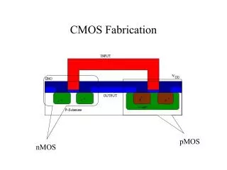
What is CMOS? • Complementary metal–oxide–semiconductor (CMOS) • Has many different uses: • Integrated Circuits • Data converters • Integrated transceivers • Image sensors • Logic circuits http://en.wikipedia.org/wiki/CMOS
What is CMOS? NAND Circuit
CMOS Fabrication ProcessOverview http://lsmwww.epfl.ch/Education/former/2002-2003/VLSIDesign/ch02/ch02.html
CMOS Fabrication Process • Create a pattern. • Oxidize small layer, about 1µm thick. • Place photoresist on top of SiO2 • Place mask(pattern) above photoresist and expose it to UV light.
CMOS Fabrication Process • Etch away SiO2 using HF acid or plasma. • Remove remaining photoresist with acids.
CMOS Fabrication Process • To create a n well: • Diffusion • Heat wafer in Arsenic gas chamber until diffusion occurs. • Ion Implantation • Arsenic or phosphorous are implanted in window.
CMOS Fabrication Process • A thin layer of oxide is deposited. • A thin layer of polysilicon is deposited using Chemical Vapor Deposition (CVD) .
CMOS Fabrication Process http://en.wikipedia.org/wiki/Chemical_vapor_deposition
CMOS Fabrication Process • Remove oxide layer using acid. • Dope open area using Ion implantation or diffusion.
Problems with Current CMOS Fabrication • Optical lithography is limited by the light frequency. • Material limitations • Yield limitations • Space limitations
Future Changes in CMOS Fabrication • Material changes like using high-k materials. • Design changes • SOI(Silicon On Insulator) • Double Gate (Finfet) • Twin-Tub Process
Future Changes in CMOS Fabrication http://www.fujitsu.com/downloads/MAG/vol39-1/paper02.pdf
References • CMOS Digital Integrated Circuit Design - Analysis and Design by S.M. Kang and Y. Leblebici • http://www.fujitsu.com/downloads/MAG/vol39-1/paper02.pdf • “Introduction to VLSI Circuits and Systems,” John Wiley and Sons, 2002 • http://lsmwww.epfl.ch/Education/former/2002-2003/VLSIDesign/ch02/ch02.html • http://en.wikipedia.org/wiki/Chemical_vapor_deposition • users.ece.utexas.edu/~adnan/vlsi-05/lec0Fab.ppt • http://en.wikipedia.org/wiki/CMOS • www.usna.edu/EE/ee452/LectureNotes/02-_CMOS_Process_Steps/08_Simple_CMOS_Fab.ppt • http://en.wikipedia.org/wiki/Silicon_on_insulator • access.ee.ntu.edu.tw/course/VLSI_design_90second/data/Chapter%203%20Part2%2003-20-2002.doc