Download
1 / 21
220 likes | 477 Views
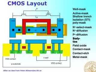
תהליך CMOS. פרופ ’ יוסי שחם המחלקה לאלקטרוניקה פיזיקלית אוניברסיטת תל-אביב ( לפי ההרצאות של יאן ראבאי מברקלי ). הכנת הפרוסות והליתוגרפיה הבסיסית. תהליך CMOS. דוגמה - מהפך CMOS. This two-inverter circuit (of Figure 3.25 in the text) will be. manufactured in a twin-well process.

E N D
תהליךCMOS פרופ’ יוסי שחם המחלקה לאלקטרוניקה פיזיקלית אוניברסיטת תל-אביב (לפי ההרצאות של יאן ראבאי מברקלי)
הכנת הפרוסות והליתוגרפיה הבסיסית
דוגמה - מהפךCMOS This two-inverter circuit (of Figure 3.25 in the text) will be manufactured in a twin-well process.
תהליך הייצור התצוגה מבוססת על התכניתSIMPL שלפרופ’ אנדי ניורייטרמאוניברסיטתברקלי. אינפורמציה מלאה נמצאת באתר: http://tanqueray.eecs.berkeley.edu/~ehab/inv.html.
Starting wafer: n-type with doping level = 10 13 3 /cm התחלה A A’ * Cross-sections will be shown along vertical line A-A’
הגדרת ה- WELL (1) Oxidize wafer (2) Deposit silicon nitride (3) Deposit photoresist
בניית ה- WELL (4) Expose resist using n-well mask
בניית ה- WELL (5) Develop resist (6) Etch nitride and (7) Grow thick oxide
בניית ה- WELL מסוגN (8) Implant n-dopants (phosphorus) m (up to 1.5 m deep)
בניית ה- WELL מסוגP Repeat previous steps
חמצון השער 0.055 mm thin
תחמוצת השדה 0.9 mm thick Uses Active Area mask Is followed by threshold-adjusting implants
פתיחת חורים (1) Deposit inter-level dielectric (SiO2) — 0.75 mm (2) Define contact opening using contact mask
מתכת 1 - אלומיניום Aluminum evaporated (0.8 mm thick) followed by other metal layers and glass