Download
1 / 21
210 likes | 378 Views
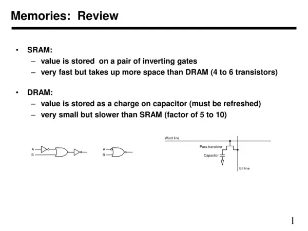
The third key component of a microprocessor-based system (besides the CPU and I/O devices). Classification Physical and external configuration Timing Types. Memories. Basic Categories. Writable? Read-Only Memory (ROM):

E N D
The third key component of a microprocessor-based system (besides the CPU and I/O devices). • Classification • Physical and external configuration • Timing • Types Memories
Basic Categories Writable? • Read-Only Memory (ROM): • Can only be read; cannot be modified (written) by the processor. Contents of ROM chip are set before chip is placed into the system. • Random-Access Memory (RAM): • Read/write memory. Although technically inaccurate, term is used for historical reasons. (ROMs are also random access.) Savable? • Volatile memories • Lose their contents when power is turned off. Typically used to store program while system is running. • Non-volatile memories do not. • Required by every system to store instructions that get executed when system powers up (boot code).
Classification ROM RAM Volatile Static RAM (SRAM) Dynamic RAM (DRAM) Non-volatile Mask ROM EEPROM PROM Flash memory EPROM BBSRAM Note that we can write some of these “ROMS”
Memory Array Mem Cell Mem Cell Mem Cell Mem Cell Why square?? Mem Cell Mem Cell Mem Cell Mem Cell word lines Mem Cell Mem Cell Mem Cell Mem Cell Mem Cell Mem Cell Mem Cell Mem Cell bit lines Different memory types are distinguished by technology for storing bit in memory cell.
Support Circuitry memory array 16 bits (4x4) A0 A1 2 to 4 decoder A2 A3 4:1 mux/demux OE# CS# WE# • Control signals: • Control read/write of array • Map internal physical array to external configuration (4x4 16x1) D0
Interface (1/2) • Physical configurations are typically square. • Minimize length word + bit line minimize access delays. • External configurations are “tall and narrow”. The narrower the configuration, the higher the pin efficiency. (Adding one address pin cuts data pins in half.) • Several external configurations available for a given capacity. • 64Kbits may be available as 64Kx1, 32Kx2, 16Kx4,…
Interface (2/2) • Chip Select (CS#): Enables device. If not asserted, device ignores all other inputs (sometimes entering low-power mode). • Write Enable (WE#): Store D0 at specified address. • Output Enable (OE#): Drive value at specified address onto D0.
tRC tAV ADDR tCS CS# tOE OE# DATA Memory Timing: Reads • Access time: Time required from start of a read access to valid data output. • Access time specified for each of the three conditions required for valid data output (valid address, chip select, output enable) • Time to valid data out depends on which of these is on critical path. • tRC: Minimum time required from start of one access to start of next. • For most memories equal to access time.
System-Level Read Timing memory CPU tabuf tadec addr buffers addr decode A CS# ADDR RD/WR# OE# tinv data buffers D D tdbuf If the CPU starts driving the address and RD/WR# at the same time, what is the access time?
Memory Timing: Writes tWC tAW ADDR tCW CS# tWP WE# tAS DATA tDS tDH • Write happens on rising edge of WE’. • Separate access times tAW, tCW, tWP specified for address valid, CS#, WE#. • Typically, tAS = 0, meaning that WE# may not be asserted before address is valid. • Setup and hold times required for data. • Write cycle time tWC is typically in the order of tAW.
Static RAM word line bit line + bit line - • Volatile memory • Each cell is basically a flip-flop • 4—6 transistors per cell relatively poor density • Very fast (access times under 1ns commonplace) • Reads/writes at same speed
Dynamic RAM word line bit line • One transistor + capacitor per cell outstanding density • Very small charges involved relatively slow • Bit lines must be precharged to detect bit values. • Reads are destructive; internal writebacks required. • Values must be periodically refreshed or charge will leak away.
tRC tAV ADDR tCS CS# tOE OE# DATA Memory Timing: Reads • Access time: Time required from start of a read access to valid data output. • Access time specified for each of the three conditions required for valid data output (valid address, chip select, output enable) • Time to valid data out depends on which of these is on critical path. • tRC: Minimum time required from start of one access to start of next. • For most memories equal to access time. • For DRAMs could exceed 2x. Why?
Mask ROM • By far the simplest technique. • Presence/absence of diode at each cell denotes binary value. • Pattern of diodes defined by mask used in fabrication process. • Contents fixed when the chip is made; cannot be changed. • Large setup cost (design mask), small marginal cost. • Good for high-volume applications where upgrading contents is not an issue. • What value is stored by presence of diode? word lines bit lines
Programmable ROM (PROM) • Replace the diode in each cell of a Mask ROM by diode + fuse (fusible-link PROM). • Initial contents are all 1s. • Users program memory by blowing fuses to create 0s. • Plug chip into PROM programmer (“burner”) device and download data file. • One-time programmable
UV Erasable PROM (EPROM) • Replace PROM fuse with pass transistor controlled by “floating” (i.e. electrically insulated) gate. • Program by charging gate to switch pass transistor. (Use special “burner” to apply high voltage that overcomes insulation.) • Erase by discharging all gates using ultraviolet light. (UV photons carry electrons across insulation.) • Insulation eventually breaks down limited number of erase/reprogram cycles (100s to 1000s). • Costly: Requires special package with window. • Largely displaced by flash memory.
Electrically Erasable PROM (EEPROM) • Similar to UV EPROM, but with on-chip circuitry to electrically charge/discharge floating gates (no UV). • Writable by CPU really a RAM despite name. • Reads/wites much like generic RAM: Internal circuitry erases affected byte/word, then reprograms to new value. • Write cycle in the order of a millisecond. • High voltage input (e.g. 12V) required for writing. • Limited number of write cycles (1000s). • Selective erasing requires extra circuitry in each memory cell Lower density and higher cost than EPROM.
Flash Memory • Electrically erasable like EEPROM, but only in large 8—128K blocks (not a byte at a time). • Erase circuitry moves out of cells to periphery substantially better density than EEPROM. • Reads much like generic RAM • Writes for locations in erased blocks: • write cycle in a few microseconds • slower than volatile RAM but faster than EEPROM • To rewrite locations, must explicitly erase entire block: • erase can take several seconds • erased blocks can be rewritten a byte at a time • Floating gate technology Erase/reprogram cycle limit (10K-100K cycles per block)
Flash Applications • Flash technology has made rapid advances in recent years. • cell density rivals DRAM; better than EPROM; much better than EEPROM. • multiple gate voltages can encode 2 bits per cell. • many-GB devices available • ROMs and EPROMs rapidly becoming obsolete. • Replacing hard disks in some applications. • smaller, lighter, faster • more reliable (no moving parts) • cost effective • PDAs, cell phones, laptops, iPods, etc…
Memories in our setup… • Internal SRAM • 26 KB Fast SRAM • Internal Flash EEPROM • 448 KB – 5 V programming • The programming power can be Enabled/Disabled via the config switches • External EPROM • U2/U3 – Holds the monitor program shipped with the board. • External SRAM • 512 KB – U4-U7 • External Flash EEPROM • 512 KB – U15/U16 (underneath the EPROMS)
Using Memories to Embed • The role of ROMs: • Every system must have boot-up code • in a ROM or battery-backed RAM • ROMs have somewhat limited write-cycles, so use them for read-only stuff like: • code • constants and static variables • The role of RAMs: • Testing and development of software (what we’re doing currently) • Storing dynamic data – anything writable. • local variables (the stack) • dynamic memory (the heap)