Download
1 / 19
190 likes | 371 Views
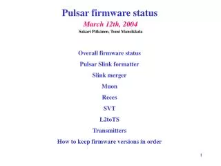
Pulsar firmware status. June 11th, 2004. Sakari Pitkänen, Tomi Mansikkala. Slink format Transmitter firmware Transmitter firmware status Receiver firmware overview Receiver firmware status New VME interface. Slink format. 8. 4. 2. 8. 8. 2. Format version. Data source. Region

E N D
Pulsar firmware status June 11th, 2004 Sakari Pitkänen, Tomi Mansikkala Slink format Transmitter firmware Transmitter firmware status Receiver firmware overview Receiver firmware status New VME interface
Slink format 8 4 2 8 8 2 Format version Data source Region ID Reserved Bunch count Buffer # Latency Data size 16 16 • Second header word added • Data size now also before data • Space for latency information Data 16 16 Data size Error flags
L1A with buffer # data latency RAM Test pattern Output FIFO data Transmitter firmware • Sends data from RAM after receiving L1A from P2 backplane connection • Has 1k or4k word internal RAM where user can load test patterns thru VME (if SRAM is used, lots of more words can be loaded) • Test pattern RAM not divided to four buffers anymore • Transmitters are able to • Have delay before sending data out • max. delay time varies between ~8.5us to ~0.5s (depends on firmware) • Have gaps between data words • Have empty events • Send same or different eventson each L1A Tomi Mansikkala
Transmitter firmware status • New transmitter firmwares • RECES TX (testing ongoing) • ISOLIST TX (testing ongoing) • MUON TX (testing ongoing) • CLIST TX (not tested yet) • XTRP TX (teststand tested, OK) • SVT TX (teststand tested, OK) • Left to do • SLINK TX • L1T TX DataIO FPGA DataIO FPGA Control FPGA Tomi Mansikkala
Receiver firmware overview Pulsar pre-processors Muon L1 muon L1 XTRP L1 trigger Slink merger TS PC L2toTS Cluster SLINK L2 CAL (CLIST/Iso) PreFred SVT SVT Reces ShowMax (RECES) Reces merger
Slink merger Four Slink mezz cards AUX card Slink output Slink inputs Status - A lot of teststand testing done - Beam tests ongoing • Receives data from four Slink inputs • Saves data to input DAQ buffers • Merges data and creates one Slink package • Saves Slink formatted data to output DAQ buffers • Sends data out from P3 - AUX card - Slink Slink merger output 0xE0F00000 Merger trailer End of fragment Input 4 trailer Slink input 4 data Input 4 header 2 Input 4 header 1 End of fragment Input 3 trailer Slink input 3 data Input 3 header 2 Input 3 header 1 End of fragment Input 2 trailer Slink input 2 data Input 2 header 2 Input 2 header 1 End of fragment Input 1 trailer Slink input 1 data Input 1 header 2 Input 1 header 1 Merger header 2 Merger header 1
Reces Four Taxi mezz cards AUX card Slink output Taxi inputs Status - Teststand testing ongoing - Ready for beam tests • Receives data from 16 Taxi fibers • Saves data to input DAQ buffers • Zero suppresses Reces data (Phase I: no zero suppresion) • Merges data and creates one Slink package • Saves Slink formatted data to output DAQ buffer • Sends data out from P3 - AUX card - Slink
Reces merger Reces 1 Reces 2 • Reces merger and Slink merger • firmwares are identical Reces merger Reces 3 Slink merger Reces merger output End of fragment Reces 3 trailer Reces Pulsar 3 data Reces 3 header 2 Reces 3 header 1 End of fragment Reces 2 trailer Reces Pulsar 2 data Reces 2 header 2 Reces 2 header 1 End of fragment Reces 1 trailer Reces Pulsar 1 data Reces 1 header 2 Reces 1 header 1 Reces merger header 1 Reces merger header 1 Slink merger output Merger trailer End of fragment Input 4 trailer Slink input 4 data Input 4 header 2 Input 4 header 1 End of fragment Input 3 trailer Slink input 3 data Input 3 header 2 Input 3 header 1 End of fragment Input 2 trailer Slink input 2 data Input 2 header 2 Input 2 header 1 End of fragment Input 1 trailer Slink input 1 data Input 1 header 2 Input 1 header 1 Merger header 2 Merger header 1
Cluster AUX card Slink output Two Taxi mezz cards Taxi inputs ISOLIST data Hotlink input CLIST data Hotlink LVDS input Hotlink mezz card Hotlink LVDS mezz card • Status • CLIST and ISOLIST inputs tested in beam • ISOLIST algorithm and Slink formatting ready for teststand testing • CLIST algorithm and Slink formatting under development • Cluster data merging under development • Receives data from 7 Taxi fibers, 6 Hotlink fibers and 1 LVDS • Saves data to input DAQ buffers • Runs algorithm on ISOLIST and CLIST data • Creates individual Slink packages for ISOLIST and CLIST data after algorithm • Merges ISOLIST and CLIST Slink formatted data • Creates one Slink package and saves it to output DAQ buffer • Sends data out from P3 - AUX card - Slink Firmware for Cluster input and algorithm done by Vadim, more on Vadim’s talk
Muon Four Hotlink Mezz cards AUX card Slink output Hotlink inputs L1T input XTRP input Status - Missing L1 trigger input - Firmware needs more work on timing optimizing and modularization - Teststand testing ongoing • Receives data from 16 Hotlink fibers, XTRP input and L1 trigger input • Saves data to input DAQ buffers • Zero suppresses Muon data • Merges Muon, XTRP and L1T data • Creates one Slink package and saves it to output DAQ buffer • Sends data out from P3 - AUX card - Slink
SVT AUX card Slink output SVX EOE input SVT input • Receives SVT data • Saves data to input DAQ buffer • Creates one Slink package • Saves Slink formatted data to output DAQ buffer • Sends data out from P3 - AUX card – Slink • Measures SVT and SVX latencies (time from L1A to BOE/EOE) • Status • - A lot of teststand testing done • Beam tests ongoing • To do • Only send data needed for L2 algorithm
L2toTS Slink mezz card Slink input CDF signals Decision L1A Buffernumber B0 Interface to TS Handshaking • Waits for L1A and data from CPU decision (or L1 trigger input) • Adjustable delay for L2 decision to TS • Sends L2A or L2R or L2TO to TS • Finishes handshake with TS and rearms for next event • Checks buffernumber and bunch count • Saves CPU decision data to DAQ RAM • Status • Teststand tests ongoing
New VME interface • One unified design that works for all firmwares • Each FPGA has two DAQ RAMs and two number of word registers (usage varies) • Each FPGA has common control and status registers (usage varies) • Registers for firmware version and DAQ software version • IDPROM on Control FPGA for each Pulsar board DataIO FPGA 1 DAQ 1 DAQ 2 DataIO FPGA 2 DAQ 1 DAQ 2 Control FPGA DAQ 1 DAQ 2
New VME interface Common address map Control FPGA Firmware version YY000000 (R) Reset YY000004 (W) DAQ SW version YY000008 (R/W) Control register 1 YY00000C (R/W) Status register 1 YY000010 (R) Pulse 1 YY000014 (W) Control register 2 YY000018 (R/W) Control register 3 YY00001C (R/W) Status register 2 YY000020 (R) IDPROM YY100000 – YY10007C (R) VME address map (user guide) YY100100 – YY1????? (R) DataIO 1 FPGA Firmware version YY080000 (R) Reset YY080004 (W) Control register 1 YY080008 (R/W) Control register 2 YY08000C (R/W) Status register 1 YY080010 (R) Pulse 1 YY080014 (W) Control register 3 YY080018 (R/W) Control register 4 YY08001C (R/W) Status register 2 YY080020 (R) VME address map (user guide) YY100100 – YY1????? (R) DataIO 2 FPGA Firmware version YY0C0000 (R) Reset YY0C0004 (W) Control register 1 YY0C0008 (R/W) Control register 2 YY0C000C (R/W) Status register 1 YY0C0010 (R) Pulse 1 YY0C0014 (W) Control register 3 YY0C0018 (R/W) Control register 4 YY0C001C (R/W) Status register 2 YY0C0020 (R) VME address map (user guide) YY100100 – YY1????? (R) Firmware version Firmware ID + Date + Version number 8-bits 20-bits 4-bits Example: Slink merger DataIO 02/20/04 first version Hex: 01402200 Firmware IDs 01 DataIO Slink merger 02 Control Slink merger 03 DataIO Muon 04 Control Muon 05 Control SVT 06 DataIO CLIST 07 DataIO ISOLIST 08 DataIO Reces 09 DataIO L2toTS 0A Control L2toTS A1 DataIO Muon TX A2 Control Muon TX A3 DataIO Reces TX A4 DataIO ISOLIST TX A5 DataIO CLIST TX A6 Control SVT TX YY = VMEaddress bits 31..24. These bits not used by firmware.
New VME interface Slink merger VME registers Control FPGA Name AddressDescription Databits Data Firmware version YY000000 (R) Firmware version 31…0 0x02405140 Reset YY000004 (W) Reset FPGA - - DAQ SW version YY000008 (R/W) DAQ SW version 31…0 Power-up value: 0 Control register 1 YY00000C (R/W) Bunch Count Shift 7…0 Power-up value: 41 Status register 1 YY000010 (R) Not used 31…0 0x00c0ffee Pulse 1 YY000014 (W) Not used - - Control register 2 YY000018 (R/W) Input selection 3…0 Power-up value: 0 (all enabled) Control register 3 YY00001C (R/W) Not used 31…0 Power-up value: 0 Status register 2 YY000020 (R) Not used 31…0 0xdeadbeef IDPROM YY100000 – YY10007C (R) IDPROM 31…24 VME address map YY100100 – YY1????? (R) Not used - - IDPROM YY100000 0 YY100004 0 YY100008 x YY10000C x YY100010 YY100014 0 YY100018 8 YY10001C 1 YY100020 YY100024 P YY100028 U YY10002C L YY100030 S YY100034 A YY100038 R Input selection YY000018 Bit 0: Input 1 Bit 1: Input 2 Bit 2: Input 3 Bit 3: Input 4 High = disable Low = enable Power-up = all enabled YY10003C YY100040 S YY100044 L YY100048 I YY10004C N YY100050 K YY100054 YY100058 M YY10005C E YY100060 R YY100064 G YY100068 E YY10006C R YY100070 YY100074 YY100078 YY10007C YY = VMEaddress bits 31..24. These bits not used by firmware.
New VME interface IDPROM IDPROM Boardtype Description 081 L2 Pulsar Muon/XTRP Rx IIa 083 L2 Pulsar SVT Road Warrior 085 L2 Pulsar Muon/XTRP/L1 Tx or SVT XTRP-emu 086 L2 Pulsar Muon/XTRP/L1 Rx IIb 087 L2 Pulsar RECES Tx 088 L2 Pulsar RECES Rx 089 L2 Pulsar Cluster/PreFred Tx 090 L2 Pulsar Cluster/PreFred Rx 091 L2 Pulsar SVT Tx 092 L2 Pulsar SVT Rx 093 L2 Pulsar Merger Tx 094 L2 Pulsar Merger Rx 095 L2 Pulsar L2TS Tx 096 L2 Pulsar L2TS 097 L2 Pulsar L1 Scaler 098 L2 Pulsar SVT TF 099 L2 Pulsar test one 100 L2 Pulsar test two 101 L2 Pulsar Stereo Tx 102 L2 Pulsar Stereo Rx YY100000 0 YY100004 0 YY100008 x YY10000C x YY100010 YY100014 0 YY100018 8 YY10001C 1 YY100020 YY100024 P YY100028 U YY10002C L YY100030 S YY100034 A YY100038 R YY10003C YY100040 S YY100044 L YY100048 I YY10004C N YY100050 K YY100054 YY100058 M YY10005C E YY100060 R YY100064 G YY100068 E YY10006C R YY100070 YY100074 YY100078 YY10007C Serial # Firmware name Board type • Part of the serial number is controlled from an on board dip switch • IDPROM VME interface is identical on all firmwares, only memory input file (.mif) needs to be firmware specific • All L2 Pulsars have been given indivitual board types
New VME interface New readout VME address map Control DAQ 1 (Pulsar output) Readout FPGA / DAQ selection bits Readout Buffer 0 YY800000 Buffer 1 YY900000 Buffer 2 YYA00000 Buffer 3 YYB00000 Word count Buffer 0 YY000800 Buffer 1 YY000900 Buffer 2 YY000A00 Buffer 3 YY000B00 FPGA selection DAQ selection VMEaddress bits 18, 19 19 18 0 0 Control 1 0 DataIO 1 1 1 DataIO 2 VMEaddress bit 17 17 0 DAQ 1 1 DAQ 2 Control DAQ 2 DAQ SW version register Readout Buffer 0 YY820000 Buffer 1 YY920000 Buffer 2 YYA20000 Buffer 3 YYB20000 Word count Buffer 0 YY000804 Buffer 1 YY000904 Buffer 2 YY000A04 Buffer 3 YY000B04 YY000008 (R/W) Please write CDF00001 into each board. Can be used as software version number. DataIO1 DAQ 1 DataIO2 DAQ 1 Readout Word count Readout Word count Buffer 0 YY880000 Buffer 1 YY980000 Buffer 2 YYA80000 Buffer 3 YYB80000 Buffer 0 YY080800 Buffer 1 YY080900 Buffer 2 YY080A00 Buffer 3 YY080B00 Buffer 0 YY8C0000 Buffer 1 YY9C0000 Buffer 2 YYAC0000 Buffer 3 YYBC0000 Buffer 0 YY0C0800 Buffer 1 YY0C0900 Buffer 2 YY0C0A00 Buffer 3 YY0C0B00 DataIO1 DAQ 2 DataIO2 DAQ 2 Readout Word count Readout Word count Buffer 0 YY8A0000 Buffer 1 YY9A0000 Buffer 2 YYAA0000 Buffer 3 YYBA0000 Buffer 0 YY080804 Buffer 1 YY080904 Buffer 2 YY080A04 Buffer 3 YY080B04 Buffer 0 YY8E0000 Buffer 1 YY9E0000 Buffer 2 YYAE0000 Buffer 3 YYBE0000 Buffer 0 YY0C0804 Buffer 1 YY0C0904 Buffer 2 YY0C0A04 Buffer 3 YY0C0B04 YY = VMEaddress bits 31..24. These bits not used by firmware.
New VME interface New readout VME address map Special case when NCHANNEL > 1 (for Cluster) DataIO1 DAQ 1 DataIO2 DAQ 1 Word count Word count Buffer 0 YY080800 Buffer 1 YY080900 Buffer 2 YY080A00 Buffer 3 YY080B00 Buffer 0 YY0C0800 Buffer 1 YY0C0900 Buffer 2 YY0C0A00 Buffer 3 YY0C0B00 Readout Readout Ch 0 Buffer 0 YY880000 Buffer 1 YY980000 Buffer 2 YYA80000 Buffer 3 YYB80000 Ch 1 Buffer 0 YY880100 Buffer 1 YY980100 Buffer 2 YYA80100 Buffer 3 YYB80100 Ch 2 Buffer 0 YY880200 Buffer 1 YY980200 Buffer 2 YYA80200 Buffer 3 YYB80200 Ch 3 Buffer 0 YY880300 Buffer 1 YY980300 Buffer 2 YYA80300 Buffer 3 YYB80300 Ch 4 Buffer 0 YY880400 Buffer 1 YY980400 Buffer 2 YYA80400 Buffer 3 YYB80400 Ch 5 Buffer 0 YY880500 Buffer 1 YY980500 Buffer 2 YYA80500 Buffer 3 YYB80500 Ch 6 Buffer 0 YY880600 Buffer 1 YY980600 Buffer 2 YYA80600 Buffer 3 YYB80600 Ch 7 Buffer 0 YY880700 Buffer 1 YY980700 Buffer 2 YYA80700 Buffer 3 YYB80700 Ch 0 Buffer 0 YY8C0000 Buffer 1 YY9C0000 Buffer 2 YYAC0000 Buffer 3 YYBC0000 Ch 1 Buffer 0 YY8C0100 Buffer 1 YY9C0100 Buffer 2 YYAC0100 Buffer 3 YYBC0100 Ch 2 Buffer 0 YY8C0200 Buffer 1 YY9C0200 Buffer 2 YYAC0200 Buffer 3 YYBC0200 Ch 3 Buffer 0 YY8C0300 Buffer 1 YY9C0300 Buffer 2 YYAC0300 Buffer 3 YYBC0300 Ch 4 Buffer 0 YY8C0400 Buffer 1 YY9C0400 Buffer 2 YYAC0400 Buffer 3 YYBC0400 Ch 5 Buffer 0 YY8C0500 Buffer 1 YY9C0500 Buffer 2 YYAC0500 Buffer 3 YYBC0500 Ch 6 Buffer 0 YY8C0600 Buffer 1 YY9C0600 Buffer 2 YYAC0600 Buffer 3 YYBC0600 Ch 7 Buffer 0 YY8C0700 Buffer 1 YY9C0700 Buffer 2 YYAC0700 Buffer 3 YYBC0700 YY = VMEaddress bits 31..24. These bits not used by firmware.