Download
1 / 37
380 likes | 629 Views
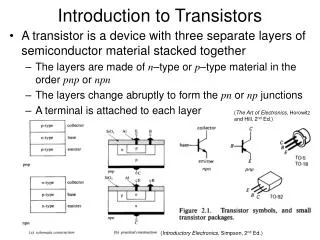
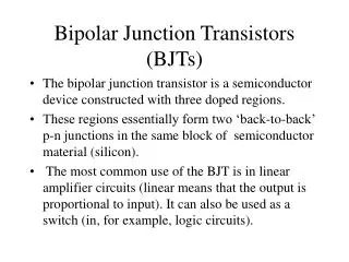
An introduction to Junction Transistors. BITX20 bidirectional SSB transceiver. A BITX20 single stage. A simplified single stage. A potential divider. An NPN Transistor. Collector. Base. Emitter. The transfer resistor (transistor). Emitter (-). Collector (+). Electrons. Base.

E N D
An NPN Transistor Collector Base Emitter
The transfer resistor (transistor) Emitter (-) Collector (+) Electrons Base Electrons are negative (Original patent used point contact)
A silicon atom (Si) Has 4 outer electrons The outer electron shell needs 8 to be “full” (standing wave pattern) Silicon will try to lend or borrow 4
An Arsenic atom (As) Has 5 outer electrons One surplus for fitting in to the lattice
A Gallium atom (Ga) Has 3 outer electrons One short for fitting in to the lattice
Gallium doping (group 3) – P type Holes are positive
What causes the depletion? • Electrons move from left to right to fill the + holes • Where electrons and holes combine the area is “depleted” of current carriers • This leaves the left (N Type) positive so eventually this prevents the depletion spreading any more. • Applying negative to N type replaces the depleted carriers and the current resumes (Forward biased diode) • Applying positive to the N type removes more electrons and increases the depletion. Almost no current flows. (Reverse biased diode)
The transfer resistor (transistor) Emitter (-) Collector (+) Electrons Base Electrons are negative (Original patent used point contact)
An alloy NPN Transistor (powered up) Depletion Emitter (-) Collector (+) Base Most alloy transistors (e.g. OC71) were germanium PNP
Characteristics of transistors • Geometry • Carrier movement • Collector “collection” efficiency (Alpha) • Asymmetry: Efficiency / Breakdown voltages • NPN transistors are normally better than PNP since electron mobility is better than hole mobility
Current gain of transistors For the original “common base” circuit the ratio of collected current to emitted current was measured. This is called Alpha. Values have improved to well over 0.99 (always less than 1). However normally we quote the current gain, called Beta. Beta = Collector current / Base current Beta values of over 200 are common.
NPN Transistor circuits • Common base • Emitter follower (common collector) • Common emitter Collector Base Emitter
Our original circuit • Potential divider bias to linear region • Partly an Emitter follower • Partly common Emitter • Voltage gain set by Collector / Emitter resistor ratios • More in a later talk Collector Base Emitter
Features of Common Emitter • High voltage gain • High current gain • Medium input impedance due to high current gain • High output impedance. For HF capacitive loading will need to be resonated reducing bandwidth. • Bad HF & bandwidth as falling beta with frequency reduces gain.
Features of Emitter followers • Voltage gain of almost exactly 1 • High current gain • High input impedance (due to high current gain) • Low output impedance (Good for unknown loads) • Good HF & bandwidth as falling beta with frequency matters less.
Features of Common Base • Current gain of approximately 1 (alpha) • Low input impedance (due to low current gain) • High output impedance (Base screens collector) • High voltage gain (if input impedance matched) • Works with a low gain transistor (beta) • Good HF & bandwidth as falling beta with frequency matters less.
A Planar NPN Transistor Collector Base Emitter
A Planar PNP Transistor on an N substrate Collector Base Emitter