Download
1 / 22
220 likes | 393 Views
INSULATORS MADE BY ECR PLASMAS ON Si or GaAs SUBSTRATES AT ROOM TEMPERATURE. J.A. Diniz, I. Doi and J.W. Swart . UNICAMP, CCS and DSIF/FEEC, CEP.13083-970, CP. 6101, CAMPINAS, SP, BRAZIL . OUTLINE CCS/DSIF/UNICAMP. MOTIVATION INTRODUCTION EXPERIMENTS RESULTS AND DISCUSSIONS

E N D
INSULATORS MADE BY ECR PLASMAS ON Si or GaAs SUBSTRATES AT ROOM TEMPERATURE J.A. Diniz, I. Doi and J.W. Swart. UNICAMP, CCS and DSIF/FEEC, CEP.13083-970, CP. 6101, CAMPINAS, SP, BRAZIL.
OUTLINE CCS/DSIF/UNICAMP • MOTIVATION • INTRODUCTION • EXPERIMENTS • RESULTS AND DISCUSSIONS • CONCLUSIONS
MOTIVATION CCS/DSIF/UNICAMP Silicon Nitrides (SiNx) and Silicon Oxynitrides (SiOxNy) on Si and GaAs N2O HIGH DENSITY PLASMA OXIDATION at low temperature ECR PLASMA DEPOSITION or OXIDATION at room temperature DEVICE ISOLATION (LOCOS) GATE DIELECTRIC • Requirement: • low effective charge density; • surface passivation • Requirement: • nitrides with high resistance to thermal oxidation ( 1000oC); • reduced bird’s beak after wet oxidation MOS devices
INTRODUCTIONCCS/DSIF/UNICAMP • Silicon nitride (SiNx) or Silicon oxynitride (SiOxNy) films • considerable attention electrical and physical properties • for enhance • MIS structuresradiation hardeningsurface passivation • Barrier against boron diffusion The improved dielectric reliability the pile up of the incorporated N in the vicinity of the SiO2/Si interface. The Si-N bonds replace the strained Si-O bonds at interface, decreasing the interface strain.
INTRODUCTIONCCS/DSIF//UNICAMP • High-density plasma techniquesECR and ICP • have been employed for • thin film (SiNx, SiOxNy and SiO2) depositions on • semiconductor substrates, such as Si and GaAs. • control separately ion energy (RF power) and ion flux (W power). • operate at low pressure (1-10 mTorr) reduce ion surface sputtering • A 2.45GHz W source generates the plasma at high power • A 13.56 MHz RF power source biases separately the sample chuck. ECR systems remote plasma reactors
ECR SYSTEM GAS INLET ECRWPOWER 2.45GHz ~ MAGNETIC FIELD 875GAUSS PLASMA GAS RING RFchuckPOWER 13.56MHz ~ VACUUM PUMP INTRODUCTIONCCS/DSIF/UNICAMP SUBSTRATE
INTRODUCTIONCCS/DSIF/UNICAMP This work - surface passivation with SiNx • SiNx films deposited on GaAs substrates • to passivate Heterojunction Bipolar Transistor (HBT) structures ;
Metal Al SiOxNy p-type Si (100) INTRODUCTIONCCS/DSIF/UNICAMP This work - plasma oxidation (without silane) • SiOxNy insulators obtained by low-energy 28N2+ implantation • (E=5keV/dose=1015cm-2) in Si substrates prior to • high density O2 ECR plasma oxidation • to gate dielectric for MOS devices; • SiOxNy insulators grown on Si by O2/N2/Ar ECR plasmaoxynitridation • to gate dielectric for MOS devices;.
INTRODUCTIONCCS/DSIF/UNICAMP This work - SiNx for isolation technology -LOCOS • SiNx films deposited on SiO2/Si structures • to verify the masking characteristics • for local oxidation of silicon process.
EXPERIMENTALCCS/DSIF/UNICAMP SiNx films deposited on GaAs substrates passivation MIS devices CN samples Al or WN E-beam or sputtering evap. SiNx Cleaned by organic solvents - Sox-let distillate C-V characteristics n-GaAs(100) n-GaAs (100) n-GaAs (100) SiNx deposited by ECR plasma N2/Ar/SiH4 (2.5/5/200sccm) 1mTorr/250WECR/1Wrf AuGeNi Ellipsometry, FTIR, profile meas. HBT I-V characteristics
EXPERIMENTALCCS/DSIF/UNICAMP SiOxNy obtained by O2/N2/Ar ECR plasma oxynitridation Cleaned by RCA method SiOxNy SiOxNy deposited or oxidized by ECR plasma p-type Si (100) p-type Si (100) 13N2/7O2/20Ar/750WECR/10WRF/4mTorr/200C DEPOSITION OXIDATION Without SiH4 With SiH4 flow of 200sccm ONCVD samples ONPO samples
EXPERIMENTALCCS/DSIF/UNICAMP SiOxNy obtained by 28N2+ implantation + plasma oxidation Cleaned by RCA method GATE DIELECTRIC OXYNITRIDE FORMATION Si -p ION IMPLANTATION 5keV N2+ Dose of 1015/cm2 WITHOUT IMPLANTATION Si -p plasma oxidation O2 flows=40sccm 500WECR 20W RF/10 mTorr 200C/30 min CTA N2/1000ºC/20min + plasma oxidation O2 flows=40sccm 500WECR 20W RF/10 mTorr 200C/30 min SiOxNy CONTROL OXIDE ONECR samples COECR samples Si -p
EXPERIMENTALCCS/DSIF/UNICAMP SiOxNy obtained on Si Physical characterization • Chemical bonding SiOxNyFTIR. • Thickness, the deposition (or oxidation) rates • and etch rates in buffered HF profile measurements Metal/oxynitride/Si capacitors SiOxNy e-beam evaporation of 150 nm thick Al film p-type Si (100) Al electrodes 200 m diameter dots. C-V measurements Electrical characterization
EXPERIMENTALCCS/DSIF/UNICAMP LOCOS Cleaned by RCA method Dry oxidation for pad oxide formation WET OXIDATION FOR ISOLATION THICK OXIDE SiNx deposited by ECR plasma SEM analysis SiO2 p-type Si (100) p-type Si (100) Ellipsometry, FTIR, profile meas. Nitride Deposition Process Parameters 200sccmSiH4/20sccmAr/5mTorr/1000WECR/1WRF/200C 20sccmN2 -N20 10 sccmN2 - N10 05sccm N2 - N5 2.5sccmN2 -N2.5 SILICON NITRIDE DEPOSITIONS samples
RESULTS AND DISCUSSIONSCCS/DSIF/UNICAMP SiNx films deposited on GaAs substrates excellent passivation LOW DR C-V Ellipsometry (nitride richs in Nitrogen) Profile meas. FTIR (Si-N and N-H bonds) Low porosity Low [H]
RESULTS AND DISCUSSIONSCCS/DSIF/UNICAMP SiNx films deposited on GaAs substrates I-V characteristics HBT an increase in current gain of over an order of magnitude the base current ideality factor reduces from 2.27 in the unpassivated device to 1.39 in the passivated HBT Excellent passivation with nitride
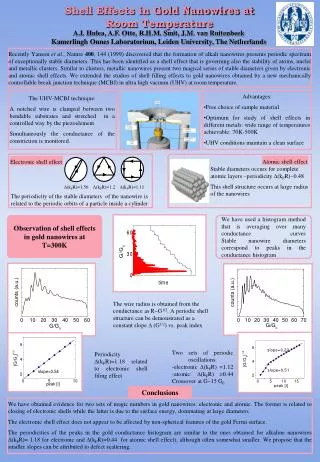
RESULTS AND DISCUSSIONSCCS/DSIF/UNICAMP SiOxNy obtained by 28N2+ implantation + plasma oxidation Charge density Control oxide oxynitride Ellipsometry (NO INHIBITION OXIDATION) C-V (high quality oxynitride) FTIR (Si-O, O-Si-N and high quality) Control oxynitride Sintering time
RESULTS AND DISCUSSIONSCCS/DSIF/UNICAMP deposited Low oxidation rate Low porosity films Ultra-thin films Plasma oxidation [H] C-V ONPO = 4.6 5nmoxynitride FTIR (Si-O and Si-O-N bonds)
RESULTS AND DISCUSSIONSCCS/DSIF/UNICAMP nitride richs in N nitride richs in Si SiNx for LOCOS Richs in Si Richs in N Ellipsometry (nitrides rich in N except to N2.5 sample) FTIR (Si-N and N-H bonds to N5,N10, N20) Profile meas. N2 flow ER Porosity [H] Ellipsometry x FTIR
RESULTS AND DISCUSSIONSCCS/DSIF/UNICAMP SiNx for LOCOS LOCOS with N2.5 Nitride For LOCOS technology, SiNx(150nm)/pad-SiO2(50nm)/Si structures were used. N2.5 nitrides were oxidized and not effective mask against oxidation Bird’s beak length of 1 mm LOCOS with N5 Nitride LOCOS with N20 Nitride high quality for LOCOS isolation technology
CONCLUSIONSCCS/DSIF/LPD/UNICAMP Oxynitrides grown by O2/N2/Ar ECR plasma oxynitridation were obtained • Characteristics: • thickness of 5.5nm • dielectric constant of 4.6, which confirms the oxynitride formation • medium breakdown E-fields of 10 MV/cm • effective charge densities of about 1010/cm2 for bombardments with doses up to 1012 protons/cm2 therefore are suitable gate insulators for MIS devices, when the proton radiation hardening is a requirement The deposited oxynitrides presented low quality as gate dielectric MOS devices.
AcknowledgementsCCS/DSIF/LPD/UNICAMP The authors would like to thank CCS/UNICAMP Staff for technical assistance, and Prof. Dr. Inés Pereyra (LME/EPUSP) for FTIR analysis. The work is supported by CNPq, AEB, FAPESP and FINEP of Brazil.