Download
1 / 1
10 likes | 87 Views
3D-FBK pixel sensors with CMS readout : first tests results

E N D
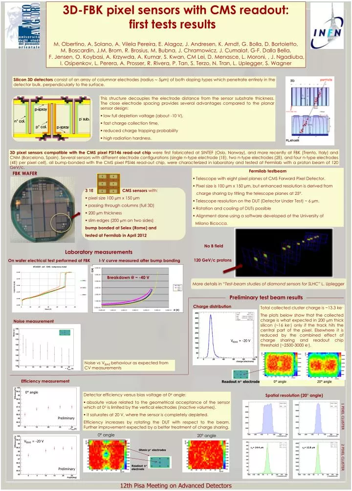
3D-FBK pixel sensors with CMS readout: first tests results M. Obertino, A. Solano, A. Vilela Pereira, E. Alagoz, J. Andresen, K. Arndt, G. Bolla, D. Bortoletto, M. Boscardin, J.M. Brom, R. Brosius, M. Bubna, J. Chramowicz, J. Cumalat, G-F. Dalla Bella, F. Jensen, O. Koybasi, A. Krzywda, A. Kumar, S. Kwan, CM Lei, D. Menasce, L. Moroni, , J. Ngadiuba, I. Osipenkov, L. Perera, A. Prosser, R. Rivera, P. Tan, S. Terzo, N. Tran, L. Uplegger, S. Wagner Silicon 3D detectors consist of an array of columnar electrodes (radius ∼ 5µm) of both doping types which penetrate entirely in the detector bulk, perpendicularly to the surface. • This structure decouples the electrode distance from the sensor substrate thickness. The close electrode spacing provides several advantages compared to the planar sensor design: • low full depletion voltage (about -10 V), • fast charge collection time, • reduced charge trapping probability • high radiation hardness. 3D pixel sensors compatible with the CMS pixel PSI146 read-out chip were first fabricated at SINTEF (Oslo, Norway), and more recently at FBK (Trento, Italy) and CNM (Barcelona, Spain). Several sensors with different electrode configurations (single n-type electrode (1E), two n-type electrodes (2E), and four n-type electrodes (4E) per pixel cell), all bump-bonded with the CMS pixel PSI46 read-out chip, were characterized in laboratory and tested at Fermilab with a proton beam of 120 GeV/c. • Fermilabtestbeam • Telescope with eight pixel planes of CMS Forward Pixel Detector. • Pixel size is 100 µmx 150 µm, but enhanced resolution is derived from • charge sharing by titling the telescope planes at 25°. • Telescope resolution on the DUT (Detector Under Test) ~ 6 µm. • Rotation and cooling of DUTs possible • Alignment done using a software developed at the University of • Milano Bicocca. FBK WAFER • 3 1E CMS sensors with: • pixel size 100 µmx 150 µm • passing through columns (full 3D) • 200 mm thickness • slim edges (200 mm on two sides) • bump bonded at Selex (Rome) and • tested at Fermilab in April 2012 No B field Laboratory measurements 120 GeV/c protons On wafer electrical test performed at FBK I-V curve measured after bump bonding I[A] Breakdown @ ~ -40 V More details in “Test-beam studies of diamond sensors for SLHC” L. Uplegger Preliminary test beam results Charge distribution Total collected cluster charge is ~13.3 ke-. The plots below show that the collected charge is what expected in 200 mm thick silicon (~16 ke-) only if the track hits the central part of the pixel. Elsewhere it is reduced by the combined effect of charge sharing and readout chip threshold (~2500-3000 e-). -V [V] Noise measurement VBIAS = -20 V Noise vs VBIAS behaviour as expected from CV measurements - Efficiency measurement Readout n+ electrode 0° angle 20° angle 0° angle • Detector efficiency versus bias voltage at 0o angle: • absolute value related to the geometrical acceptance of the sensor which at 0o is limited by the vertical electrodes (inactive volumes). • it saturates at 20 V, where the sensor is completely depleted. • Efficiency increases by rotating the DUT with respect to the beam. Further improvement expected by a better treatment of charge sharing. Spatial resolution (20° angle) 1 PIXEL CLUSTER Preliminary - 0° angle 20° angle VBIAS = -20 V sx= 14.4 mm sy= 12.8 mm Ohmicp+ electrodes 2 PIXEL CLUSTER Readoutn+ electrode Preliminary 12th Pisa Meeting on Advanced Detectors