Download
1 / 38
620 likes | 1.11k Views
1. -. D. 2. -. D. 3. -. D. 1887. 1987. p. e. r. i. o. d. i. c. i. n. p. e. r. i. o. d. i. c. i. n. p. e. r. i. o. d. i. c. i. n. o. n. e. d. i. r. e. c. t. i. o. n. t. w. o. d. i. r. e. c. t. i. o. n. s. t. h. r. e. e. d. i.

E N D
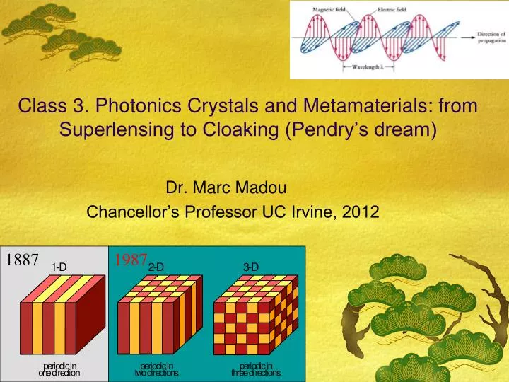
1 - D 2 - D 3 - D 1887 1987 p e r i o d i c i n p e r i o d i c i n p e r i o d i c i n o n e d i r e c t i o n t w o d i r e c t i o n s t h r e e d i r e c t i o n s Class 3. Photonics Crystals and Metamaterials: from Superlensing to Cloaking (Pendry’s dream) Dr. Marc Madou Chancellor’s Professor UC Irvine, 2012
Looking Ahead • Photonics involves the use of radiant energy, and uses photons the same way that electronic applications use electrons. • With photons traveling much faster than electrons, photonics, potentially, offers an effective solution to faster circuits by implementing optical communication systems based on optical fibers and photonic circuits. • Unfortunately traditional optical waveguides involves structures that cannot be made much smaller than λ/2 because of diffraction. • Furthermore, waveguiding along bent guides is very lossy . The latter problem is overcome in photonic bandgap structures. But the dimensions of the structures are still limited by the wavelength of light. • The hot new photonic topic that might solve the size and bending problem and that is plasmonics .
Looking Ahead • Surface plasmon–based circuits: Waveguiding of plasmonic excitation in closely placed metal nanoparticles ( today way too lossy!). • This class: • We start this class by categorizing natural crystals and metamaterials, photonic crystals and geometric optics (a vs. ). • We then consider in more detail photonic crystals and metamaterials and explore applications for both. • We also present a comparison table of electrons with photons.
Contents • From crystals and metamaterials to photonic crystals and geometric optics: a matter of repeat size a vs. . • Photonic Crystals. • Photonic Crystal Applications. • Photons vs. Electrons. • Metamaterials. • Metamaterial Applications: • Superlenses • Cloaking.
From Crystals and Metamaterials to Photonic Crystals and Geometric Optics • Material properties are determined by the properties of their sub-units with their spatial distribution. Electromagnetic properties as a function of the ratio a the “lattice constant” of the material/structure and λ the wavelength of the incoming light (a/) can be organized in three large groups: • Natural crystals (violet Tanzanite in the figure further below) and metamaterials have lattice constants much smaller than the light wavelengths: a << λ. These materials are treated as homogeneous media with parameters ε and μ (which are tensors in anisotropic crystals). They either have a positive refractive index: n > 1, and show no magnetic response at optical wavelengths (μ = 1) in natural crystals or they have a negative refractive index in metamaterials (manmade).
From Crystals and Metamaterials to Photonic Crystals and Geometric Optics • When a is in the same range of the wavelength of the incoming light one defines a photonic crystal; a meso-scale material with subunits bigger than atoms but smaller than the EM wavelength. In photonic crystals a is the distance between repeat units with a different dielectric constant, so we can still call it “lattice constant”. Photonic crystals have properties governed by the diffraction of the periodic structures and may exhibit a bandgap for photons. They typically are not described well using effective parameters ε and μ and may be artificial or natural (in the figure that follows we show an artificial 3D photonic crystal and peacock feathers as an example of natural photonic crystals). • When considering macroscopic optic components with a critical dimension a >>>λ, geometric optics do apply. In this case a might be the repeat unit of a grating, the aperture of a lens or the length of a side of an optical triangular prism.
Photonics Crystals • A breakthrough in photonics in 1987 was the proposal of photonic crystals, with periodicity of the refractive index n in two or three dimensions (2D and 3D) (Sajeev John, Eli Yablonovitch). A 1D “photonic crystal” had been known since 1887 (a Bragg mirror). • The dispersion character of light in a bulk medium with a uniform refractive index, n was analyzed in class 2 (see also figure). • The dispersion curve of a 1D “photonic crystal” deviates from the straight-line dispersion curve of a uniform bulk medium.The region of kz between –π/a and π/a is called the First Brillouin zone. 'Yablonovite', Eli Yablonovitch's first photonic band-gap structure
Photonics Crystals • The principle of the 1D “photonic crystal” can be understood as follows. Each interface between two consecutive materials contributes a Fresnel reflection. • For the design wavelength, the optical path length difference between reflections from subsequent interfaces is half the wavelength; in addition, the reflection coefficients for the interfaces have alternating signs. Therefore, all reflected components from the interfaces interfere constructively, which results in a strong reflection. The reflectivity achieved is determined by the number of layer pairs and by the refractive index contrast between the layer materials. • A semiconductor cannot support electrons of energy lying in the electronic band gap. Similarly, a photonic crystal cannot support photons lying in the photonic band gap. By preventing or allowing light to propagate through a crystal, light processing can be performed.
Photonic Crystals • Before 1987, one-dimensional photonic crystals in the form of periodic multi-layers dielectric stacks (such as the Bragg mirror) were studied extensively. Lord Rayleigh started their study in 1887, by showing that such systems have a one-dimensional photonic band-gap, a spectral range of large reflectivity, known as a stop-band. • The 1987 definition of a “photonic crystal” has two requirements: high index contrast and a 2D or 3D periodic structure (1D is often excluded).
Photonic Crystals • Compared to 1D “photonic crystal”, it is relatively more difficult to deduce the dispersion curves for 2D and 3D photonic crystals. The software for doing this is publicly available at: http://www.elec.gla.ac.uk/groups/opto/photoniccrystal/Software/SoftwareMain.htm. • Complete photonic band gaps can only be obtained under favorable circumstances, i.e., with the right structures and sufficient (threshold) refractive index contrast. The threshold refractive index contrast for complete band gaps in 3-D photonic crystals depends on the exact structure, for diamond, for example, it is 1.87 and for an inverse opal structure it is 2.80. • Similar to the periodic electron-crystal lattice, one can fabricate photonic-crystal lattices. The refractive index varies with a much larger period of around 200 nm.
frequency (c/a) 11% gap for gap at l = 1.55µm, sphere diameter ~ 330nm Photonic Crystals:The First 3d Bandgap Structure (theoretical) Overlapping Si spheres K. M. Ho, C. T. Chan, and C. M. Soukoulis, Phys. Rev. Lett.65, 3152 (1990).
Photonic Crystals • In spite of successes in the microwave range (Yablonovite), it took over a decade to fabricate photonic crystals that work in the near-infrared (780-3000 nm) and visible (450-750 nm) regions of the spectrum. • The main challenges were to find suitable materials and processing techniques to fabricate structures that are about a thousandth the size of the microwave crystals.That is where MEMS came in (e.g., porous Si)
Photonic Crystals • Nature is way ahead of the scientists, the iridescence of various colorful living creatures, from beetles to peacock feathers to butterflies, are due to photonic crystals. • Unlike pigments, which absorb or reflect certain frequencies of light as a result of their chemical composition, the way that photonic crystals reflect light is a function of their physical structure. • These natural photonic crystals can lead to shifting shades of iridescent color that may help some animals attract mates or establish territories.
Photonic Crystals • Most proposals for devices that make use of photonic crystals do not use the properties of the crystal directly but make use of defect modes. • Such a defect is made when the lattice is changed locally. As a result, light with a frequency inside the bandgap can now propagate locally in the crystal, i.e. at the position of the defect. It is however still impossible to propagate in the surrounding photonic crystal material. • 100% transmission at sharp bends is possible.
Photonic Crystals • A photonic band gap (PBG) crystal is a structure that could manipulate beams of light in the same way semiconductors control electric currents. • In photonic crystals photons with energy in the energy bandgap can still move through lattice defects regions • Devices remain large though, for small photonic devices plasmonics are better. The latter, at least today, unfortunately come with very large losses.
Photonic Crystal Applications • Super refraction: The prism effect refers to separation of colors by refraction through a prism. • The dispersion or variation of refractive index with wavelength, i.e., the derivative (dn/dλ) of the refractive index with wavelength is low. • In a normal bulk medium like glass, dispersion is small, but dn/dλ can be made unusually large in photonic crystals.
Photonic Crystal Applications • Photonic crystal optic fibers are a special class of 2D photonic crystals where the dimension of the medium perpendicular to the crystal plane could be 100s of meters long. These are known by several names: photonic crystal fiber, photonic bandgap fiber, holey fiber, microstructured fiber and Bragg fiber. • The central defect (missing hole in the middle-5 µm across) acts as the fiber's core. The fiber is about 40 microns across. • Photonic band gap fiber: guiding light in air. Bragg fiber using perfect cylindrical dielectric mirrors (the Omniguide fiber).
Photonic Crystal Applications • Applications of photonic crystals: • Better lasers • Optical insulators • Perfect dielectric mirrors • Better LEDs • Polarizers • Better optical filters • Micron size optical benches • Photonic diodes and transistors • Jewellery • Negative refractive index (see also metamaterials) • Superlensing
Photonic Crystal Applications:PBG Laser • The smallest defect mode laser is shown ( Axel Scherer, California Institute of Technology). • Periodic air holes in high index material forms a 2D photonic crystal. • The center air hole is removed and forms a resonant cavity. Light is confined in the cavity. • Spontaneous emission in the band gap is prohibitted, but for the defect mode is enhanced. • This produces a microlaser with very low threshold. PBG Defect Laser
Metamaterials • We now delve into the fascinating new topic of metamaterials, man-made structures with a negative refractive index • This could make for perfect lenses and cloaking and might change the photonics field forever. Pendry
Metamaterials • In vacuum and for most materials the “right-hand rule” relates E, H, and k because normally μ > 0 and ε > 0. Thy are right-handed materials (RHM), • But in 1968, Victor G. Veselago postulated that if the permittivity ε and permeability μ of materials are negative simultaneously, there is no violation of any fundamental physical rules and the materials will have special optical properties. For a material with µ and negative, the vectors E and H and k form a left set of vectors and one refers to them as Left-Handed Materials (LHMs) • See also our earlier statements about S and k.
As no naturally occurring material or compound has ever been demonstrated with both ε and μ negative , Veselago (1968) wondered whether this apparent asymmetry in material properties was just happenstance, or perhaps had a more fundamental origin. From 1996 on strong theoretical and experimental evidence started emerging (Pendry) that Left-Handed Materials, now called metamaterials, could be fabricated (at least in the rf range but not yet in the optical range). Most materials do come with ε > 1 (e.g., ε = 12 for Si), but this is not without exceptions; we know that materials with a negative ε at optical frequencies (visible, IR) include metals such as Au, Ag and Al. Most materials have µ ≈ 1 and they are non-magnetic but if µ ≠ 1, one deals with a magnetic material. With µ >1 we have a paramagnetic material at hand and with µ <1, it is diamagnetic and finally with µ>>1 we define a ferromagnetic material. Materials with a negative µ are again the exception, they include resonant ferromagnetic or antiferromagnetic systems at microwave frequencies. Metamaterials
Metamaterials • Refraction: The direction of the refracted light bends away from the normal to the interface between two media, rather than toward the normal, as in Snell's Law (see also meta water above) • First microwave were shown to exhibit negative refractive index (at around 10.5 GHz) on a metamaterial with wire and spit ring resonators on the same substrate. Today we are close to the optical range.
Conventional lenses need a wide aperture NA for good resolution but even so they are limited in resolution by the wavelength employed. The contribution to the image from the far field are limited by the free space wavelength λ0. From θ = 90° (see Abbe ‘limit), we get a maximum value of the wavevector kx = k0= ω/c0=2π/λ0 − the shortest wavelength component of the image. Hence the resolution R is no better than: Contributions of the near field to the image come from large values of kx responsible for the finest details in the source. But in the near field the familiar ray diagram do not work since: ‘Near field’ light decays exponentially with distance away from the source. The missing components of a traditional far field image are thus contained in the near field and this field decays exponentially and cannot be focused in the normal way. Superlenses
It is here that Pendry, again, had an amazing insight : he suggested that a super lens can be made from a flat slab of negative refractive index material which not only brings rays to a focus but has the capacity to amplify the near field so that it can contribute to the image thus removing the wavelength limitation. Let us compare imaging with a traditional and a “Vesalago” lens. A negative refractive index medium (LH) bends light to a negative angle relative to the surface normal. Light formerly diverging from a point source is set in reverse and converges back to a point. Released from the medium the light reaches a focus for a second time. The new Pendry lens based on negative refraction has unlimited resolution provided that the condition n = −1 is met exactly. This can happen only at one frequency. So the secret of the new lens is that it can focus the near field and to do this it must amplify the highly localised near field to reproduce the correct amplitude at the image. This can be understood from the Fermat principle that light takes the shortest optical path between two points as illustrated further below. For a traditional lens the shortest optical distance between object and image is: Superlenses
Light enters n > 0 material deflection Light enters n < 0 material focusing For a perfect lens the shortest optical distance between object and image is zero: n1d1+n2d2+n1d3=0= n1d'1+n2d'2+n1d'3 RH RH LH RH RH RH n=1 n=1.3 n=1 n=1 n=-1 n=1 Superlenses
Superlenses • Both paths converge at the same point because both correspond to a minimum. In the Pendry lens, n2 is negative and the ray transverses negative optical space. • A super-lens prevents image degradation and beats the diffraction limit established by Abbe! However the resonant nature of the amplification places sever demands on materials: they must be very low loss!
Superlenses • In other words for a perfect lens the image is the object. The evanescent waves are re-grown in a negative refractive index slab and fully recovered at the image plane as illustrated in this figure.
Superlenses • A poor’s man near-field superlens (e<1 and m=1) has already been demonstrated. In 2003, Zhang's group at UC Berkeley, showed that optical evanescent waves could indeed be enhanced as they passed through a silver superlens. • They took this work one step further and imaged objects as small as 40-nm across with blue light at 365 nm with their superlens, which is just 35-nm thick. With the superlens, using 365 nm illumination features of a few tens of 10 nm were imaged, clearly breaking Abbe’s diffraction limit.
Cloaking • Pendry proposed to build a special material that wraps around an object and which would 'grab' light heading towards it and make it flow smoothly around the object rather than strike it. To an observer the light would appear to have behaved as if there was nothing there. • Thus no light strikes the object, nor does the object cast any shadow. It is completely invisible. • Diagram created by Dr. David Schurig. The cloak deflects microwave beams so they flow around a "hidden" object inside with little distortion, making it appear almost as if nothing were there at all.
Metamaterials • Today cloak only works in 2D and only with microwaves of a specific wavelength. • Making something invisible to the human eye would present a much greater challenge. • It is not very likely that this technology would work in the visible.