Download
1 / 8
100 likes | 327 Views
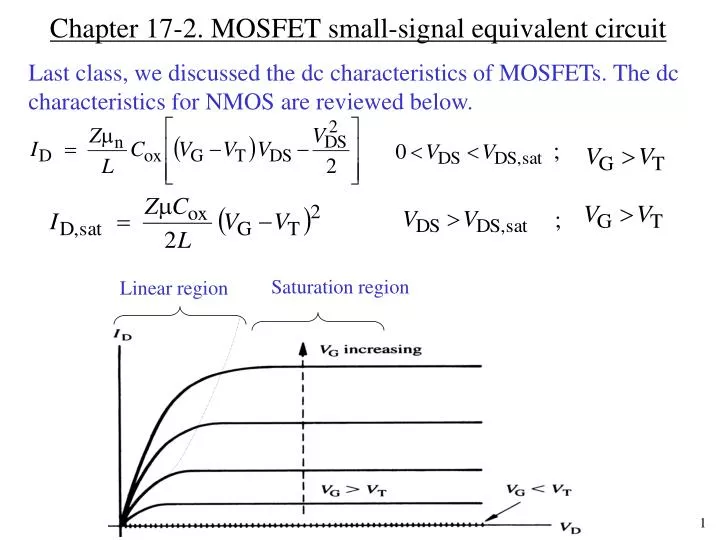
Chapter 17-2. MOSFET small-signal equivalent circuit. Last class, we discussed the dc characteristics of MOSFETs. The dc characteristics for NMOS are reviewed below. ;. ;. Saturation region. Linear region. MOSFET ac response. MOSFET ac response is routinely expressed in terms of small-

E N D
Chapter 17-2. MOSFET small-signal equivalent circuit Last class, we discussed the dc characteristics of MOSFETs. The dc characteristics for NMOS are reviewed below. ; ; Saturation region Linear region
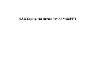
MOSFET ac response MOSFET ac response is routinely expressed in terms of small- signal equivalent circuits. This circuit can be derived from the two-port network shown below: G D MOSFET input output S S The input looks like an open circuit, except for the presence of the gate capacitor. At output, we have a current ID which is controlled by VG and VDS. ID = f (VG, VDS )
MOSFET small-signal equivalent circuit Any ac signal in VG or VDS will result in corresponding ac variation in ID and where gm = trans-conductance gd = drain or channel conductance Note: id,vg and vd are small-signal ac currents and voltages. They are different from ID, VG and VDS which are dc currents and voltages.
Small-signal equivalent circuit So, the equivalent circuit at low-frequency looks like (neglecting the gate capacitance low frequency): For high-frequency, we have to include the capacitive effects:
MOSFET small-signal parameters When VDS < VDS,sat (i.e., below pinch-off or linear region) When VDS > VDS,sat (i.e., above pinch-off or saturation region) gd = 0 Note: the parameters depend on the dc bias, VG and VDS
Frequency response of MOSFET The cut-off frequency fT is defined as the frequency when the current gain is 1. vGhere is ac signal CGS is approximately equal to the gate capacitance, Z L Cox Input current = Output current = So, at fT, So,
CG-VG characteristics: MOS-C versus MOSFET CG vs. VG characteristics of a MOSFET at high frequency looks similar to the low-frequency response (unlike the MOS-C). This is because, even at high frequency, the source and drain can supply the minority carriers required for the structure to follow the ac fluctuations in the gate potential when the device is inversion biased. CG vs. VG characteristics of a MOSFET with VDS = 0
Enhancement mode MOSFETs The devices we discussed so far are called “enhancement-mode MOSFETs. For NMOS, VT is positive and one has to apply a positive gate voltage to turn on the device. At zero gate voltage, the device will be off. For PMOS, VT is negative and one has to apply a negative gate voltage to turn on the device. At zero gate voltage, the device will be off. Exercise: Draw the ID-VDS characteristics for NMOS and PMOS enhancement-mode devices. Next class, we will discuss depletion-mode devices.