Download
1 / 20
200 likes | 365 Views
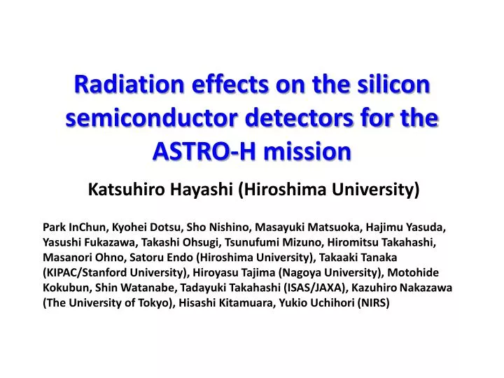
Radiation effects on the silicon semiconductor detectors for the ASTRO-H mission. Katsuhiro Hayashi (Hiroshima University).

E N D
Radiation effects on the silicon semiconductor detectors for the ASTRO-H mission Katsuhiro Hayashi (Hiroshima University) Park InChun, KyoheiDotsu, Sho Nishino, Masayuki Matsuoka, Hajimu Yasuda, Yasushi Fukazawa, Takashi Ohsugi, Tsunufumi Mizuno, Hiromitsu Takahashi, Masanori Ohno, Satoru Endo (Hiroshima University), Takaaki Tanaka (KIPAC/Stanford University), Hiroyasu Tajima (Nagoya University), MotohideKokubun, Shin Watanabe, Tadayuki Takahashi (ISAS/JAXA), Kazuhiro Nakazawa (The University of Tokyo), HisashiKitamuara, Yukio Uchihori (NIRS)
The ASTRO-H mission HXT ASTRO-H • 6th Japanese X-ray satellite • Scheduled to be launched in 2014 • 4 observation systems SGD HXI
HXI/SGD hard X-ray • Multi layers of strip-type sensors • Hybrid structure of Si (5—30 keV) and CdTe (30—80 keV) Si HXI CdTe • Narrow field of view Si/CdTe Compton camera • Si: good scatterer to determine the photon direction by the Compton kinematics SGD Surrounded by BGO crystal lower the background level
HXI/SGD hard X-ray • Multi layer of strip-type sensors • Hybrid structure of Si (5—30 keV) and CdTe (30—80 keV) Si HXI CdTe • Si/CdTe Compton camera • Narrow field of view • Si: good scatterer to determine the photon direction by the Compton kinematics SGD detectable sensitivity Suzaku/HXD Flux (ph/s/keV/cm2) SGD HXI Surrounded by BGO crystal lower the BGD level 4 Energy (keV)
DSSD (for HXI) • Utilized for HXI • DC-coupled electrode n-strip is surrounded by atoll-shaped p-stop for localization of each strip
DSSD (for HXI) • Utilized for HXI • DC-coupled electrode Improved configuration DC coupled Al electrode is attached on the p-stop to reduce the Johnson noise by the resistance • n-strip is surrounded atoll-shaped p-stop for individualization of each strip
Si-pad (for SGD) readout electrode • Pixel-array-type Si sensor • DC-coupled electrode • Signal is brought out by a readout electrode on the sensor • Improved configuration • Increase the thickness of SiO2 layer (1um1.5um) readout electrode SiO2 Si
Basic performance of DSSD • Leakage current vsbias voltage • 241Am spectrum (-15 deg) • Energy resolution @60 keV (FWHM) TestPulse 60keV
Basic performance of Si-pad • Leakage current vsbias voltage • 241Am spectrum (-15 deg) • Energy resolution @60keV (FWHM) 20℃ 0℃ Leakage current (pA) -20℃ Bias voltage(V)
Basic performance of DSSD and Si-pad is satisfied with the requirements • In the orbit of ASTRO-H, the sensors suffers radiation damage about 1krad/year Proton and 60Co γ-ray irradiation tests were performed for the DSSD and Si-pad with some improved structures
Proton Irradiation Si-pad Proton beam DSSD
Leakage current (-15℃) Si-pad DSSD after after before before α=current/fluence (damage constant) • Leakage current on the spot area increased by • ~10 pA/strip (DSSD) and ~40 pA/pad (Si-pad) • Low current increase of DSSD • limited spot region (φ~1cm) for the irradiated strip • α = 2.2x10⁻⁸(nA/cm) (Si-pad) • almost consistent with other Si sensor measurements (e.g; Ohsugi et al. 1988) DSSD Φ~1cm spot size Si-pad
60Co γ-ray irradiation Leakage current after irradiation (Si-pad) 60Co Si-pad DSSD
Dose vs. Leakage current (-15℃) DSSD Si-pad • Leakage current became larger as the dose level increased. • ~90 pA/strip (DSSD-Pside) and ~40 pA/pad (Si-pad) (10 krad) • Increase of the leakage current is 0.13nA/cm2/krad (DSSD-Pside) • consistent with that of other measurements of the micro-strip sensors for GLAST (0.11nA/cm2/krad)
Defect of trap level (gamma-ray irradiation) DSSD Si-pad Defect of trap level (Et-Ei) Et (0krad) Et (10krad) Ei Eg Et-Ei lowered new trap level is created by the irradiation and becomes dominant source of the leakage current
Effect on the noise level • Noise level is due to the leakage current, capacity and resistance of the detector and electronic circuit Shot noise • Leakage current affects the noise performance as the shot noise • Noise level (-15deg) meets the requirement of < 2 keV and is not significantly change
Summary • We have developed Si sensors (DSSD and Si-pad) utilized for the X-ray observatory ASTRO-H • Basic performance of the Si sensors meets the requirements for the mission • Proton and gamma-ray irradiation testfor the Si sensors were performed in order to evaluate the irradiation damage • Leakage current level became larger by 40--90 pA/strip(pad), which is almost consistent with other measurements of Si sensor • From the noise level, radiation effects are not significant under the operation temperature for 10 years orbits
Improvement configurations • Noise level lowered by attached Al electrode on the p-stop for n-strip of DSSD before after • Capacitance of dependency of readout electrode length is lowered by increase of the thickness of SiO2 layer for Si-pad capacitance (pF) readout electrode length (cm)
Radiation effect on the Si sensor • In the orbit of ASTRO-H, the sensors suffers radiation damage mainly by the cosmic-ray protons with the level of ~1 krad per year • Surface damage • Holes generated in the surface SiO2 • layer is trapped in the defects close • to the interface Accumulation of • positive charge in the SiO2 layer • Bulk damage • Lattice atoms are displaced from • original lattice position by interaction with high energy particles • These defects create energy levels in the forbidden band and leakage current increases noise level increase • Carry out irradiation test to evaluate effect on the DSSD and Si-pad with some improvement configurations Gamma-ray, Particle SiO2 h defect crystal h h h h Si+ Si+ Si+ Si High energy particle Si