Download
1 / 49
500 likes | 721 Views
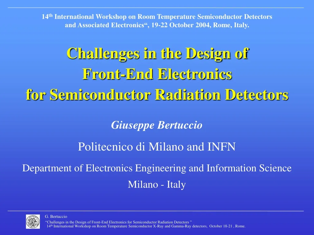
14 th International Workshop on Room Temperature Semiconductor Detectors and Associated Electronics“, 19-22 October 2004, Rome, Italy. Challenges in the Design of Front-End Electronics for Semiconductor Radiation Detectors. Giuseppe Bertuccio.

E N D
14th International Workshop on Room Temperature Semiconductor Detectors and Associated Electronics“, 19-22 October 2004, Rome, Italy. Challenges in the Design of Front-End Electronics for Semiconductor Radiation Detectors Giuseppe Bertuccio Department of Electronics Engineering and Information Science Milano - Italy Politecnico di Milano and INFN
The design challenges start from the detector A stimulating case… Silicon Carbide Detectors …a step forward for Front-end Electronic Design (useful also for other detectors…) Introduction The Front-End Electronics is made for a detector
Si / GaAs 1 nA/cm2 Leakage Current Density State of the art detectors
Si / GaAs 1 nA/cm2 SiC 1 pA/cm2 1000 Leakage Current Density State of the art detectors
Si / GaAs 1 nA/cm2 SiC 1 pA/cm2 Leakage Current Density State of the art detectors 1000
SiC pixel detector: from 27 °C to 100°C 43 e- r.m.s. @ 100 °C 17 e- r.m.s. @ 27 °C Front-End limited
SiC Pad detectors : JSiC = 1 – 10 pA/cm2 Current of a pixel ? Area = 400 x 400 mm2 IREV = 1.6 fA - 16 fA ! VBIAS=0V; I = 0 ± 0.1 fA SiC Pixel Detectors 4x4 Prototype SiC pixel 400 x 400 mm2
SiC Pad detectors : JSiC = 1 – 10 pA/cm2 Current of a pixel ? Area = 400 x 400 mm2 IREV = 2 fA - 16 fA ! VBIAS=200V; I = 3.16 ± 0.3 fA VBIAS=0V; I = 0 ± 0.1 fA Pixel Leakage Current 4x4 Prototype SiC pixel 400 x 400 mm2
June 2004 : Reverse Current Map Leakage CurrentE.N.C. @ 27 °C@ 10ms I = 274 fA : 1 pixel = 5.8 e- I = 98 fA : 1 pixel = 3.5 e- I = 36 fA : 1 pixel = 2 e- I < 10 fA :12 pixels < 1 e- r.m.s. Leakage Current @ 27 °C I = 274 fA : 1 pixel I = 98 fA : 1 pixel I = 36 fA : 1 pixel I < 10 fA : 12 pixels 10 fA I < 10fA : 12 pixels I < 10fA : 12 pixels < 1 e- r.m.s. SiC pixel A Room Temperature Sub-electron noise Semiconductor Detector
Some questions… Is it realistic to think to a sub-electron noiseroom temperature Front-End Electronics ? Is it possible sub-e-noise in standard CMOS Technology ? If not, what is the ultimate noise limit ? 1, 2 , 5… electrons r.m.s. ? What does set the noise limit in CMOS ? 1/f or others ? What is the power level required to achieve the ultimate noise ? Is this power compatible with a thousand channels pixel detectoror it is reasonable only for few channels detectors ?
Front End Noise E. Gatti, V. Radeka, P.F. Manfredi, M. Sampietro, V. Re, A. Pullia, P. O’Connor, G. De Geronimo, G. Bertuccio…
1 / f Noise outline • The classical theory and its limits • 1/f noise : models and experiments • Optimisation of ENC1/f • Ultimate limit of ENC1/f
Assumptions • Sv is independent by I • Sv scales with (WL)-1 Capacitive Matching ENC 1/f: the classical theory Are these assumptions always true ?
!? DSV/SV ~ 100 % ! SV: Experimental data PMOS 30/2 ( AMS 0.35 mm ) 10 mA 30 mA 100 mA 300 mA 1/f
N : carriers numbers v : carrier velocity Models of 1/f noise 1. Hooge model : Dm 2. McWhorter model : DN 3. Unified - correlated model : DN - Dm 1. Hooge model : Dm 2. McWhorter model : DN 3. Unified - correlated model : DN - Dm
1/f origin: m - fluctuations due to phonon scattering Dm : Hooge model - Empirical model - Proposed by Hooge in 1969 to explain 1/f noise in homogeneous semiconductors (resistors)
N - DN N - dq Si Si SiO2 SiO2 DN : McWhorter model • Based on a model proposed by McWhorter in 1957 • Fluctuation of number offree carriers 1/f origin in MOSFET DN due to charge trapping / detrapping in SiO2
SI : Dm vs. DN model DN Dm Subthreshold Ohmic Saturation
p –MOSFET 10/10 (Lmin= 90 nm) Subthreshold SII 2 DN model (McWhorter) Valenza et al. IEE 2004 Dm vs. DN models DN Dm Subthreshold
p –MOSFET 10/10 (Lmin= 90 nm) Dm (Hooge) model Saturation SI (VGS - VT)3 Valenza et al. IEE 2004 Dm vs. DN models DN Dm Saturation
saturation Dm Hooge model DN - McWhorter model I Dm vs. DN : experimental ST Microelectronics 0.13 mmCMOS PMOS NMOS Marin et al. - IEE 2004
Dm vs. DN model PMOS : deeper channel → bulk effect → Dm NMOS: interface channel → trapping effects →DN
SV SV SV Dm DN I I Dm vs. DN ENC optimisation DN Dm Saturation SI
ENC1/f : DN model: Saturation • independent by I • same for equal area WL • minimum for CG = CIL
3 e- 1 0.5 pF 50 fF Ultimate limit of ENC1/f
In contrast with series white noise minimisation minimum current (within saturation) constant current minimum for CG = 3 CIL minimum for CG = CIL Dm model: ENC1/f
CG = 3 CIL CG = CIL/3 ENC2 ws 1/f 1/f ws I CG COPT Iopt 3CIL 1/3CIL ENC optimisation 1/f White
Iopt = 14 mA Wopt = 183 mm ENCmin = 2.8 e- r.m.s. ENC [electrons r.m.s. ] Current [A] 183 Gate width W [mm] 14 mA ENC optimisation CIL =0.3 pF t = 10 ms PMOS AMS 0.35 mm aH=4.6 10-5
Summary - Conclusions • RT detectors with sub-electron noise (SiC) • Ultimate limit of CMOS Front End • 1/f noise models revised • McWhorter model limits • Hooge & unified models • Bias dependent 1/f noise • Bias Current / Geometry MOSFET optimisation • ENC1/f :1 - 3 e- r.m.s. at RT for CIL 50-500fF • ENCtot = 3 e- r.m.s. (CIL = 0.3pF )experimental data based
Acknowlegments Thanks to: Andena Marco Caccia Stefano Maiocchi Diego Mallardi Enzo Masci Sergio Olivieri Gianluigi
Intrinsic detector noise Si GaAs CdTe SiC 6 4 1 30 60 eV 1 keV Sub-electron noise Front End : is it interesting ?
Parallel noise: MOSFET Gate leakage 90 nm Technology tox = 1.5 nm PMOS 0.3/10 100 nA ID IG 1 nA Valenza et al. IEE 2004
AMS CMOS 0.35 mm PMOS 300/0.4 ID = 5 mA ID= 20 mA AMS CMOS 0.35 mm tox = 7.6 nm
1/f ENC component CIL =0.3 pF t = 10 ms PMOS AMS 0.35 mm aH=4.6 10-5 Iopt = 1 mA Wopt = 570 mm ENCmin = 1.4 e- r.m.s. ENC [electrons r.m.s. ] 570 Current [A] Gate width W [mm] 1 mA
White series CIL =0.3 pF t = 10 ms PMOS AMS 0.35 mm aH=4.6 10-5 Iopt = 10 mA Wopt = 60 mm ENCmin = 0.8 e- r.m.s. ENC [electrons r.m.s. ] 10 mA Current [A] Gate width W [mm] 60
m ± Dm , N - DN m , N - Si Si SiO2 SiO2 Unified model : correlated Dm - DN • Proposed by Mikoshiba in 1982, developed in 1987-91 • Trapping (DN) & mobility (Dm) fluctuations correlation
Implemented in SPICE BSIM3 Unified model : correlated Dm - DN Magnitude N & asc determines DN or Dm dominance
Floating gate amplifier - multiple non destructive readings T = - 110 °C Processing time 160 ms = ( 16 readings ) x 10 ms » NIM A361 (1995) 55Fe 120 eV FWHM 1 0.9 e- r.m.s.
Wide Bandgap EG=3.2 eV High Critical Field EC = 2 MV/cm High thermal conductivity SiC properties High saturation velocity vS = 200 mm/ns l SiC l Si
PMOS 6.5 e - 3.5 e - 1 1pF AMS PMOS: Lmin= 0.35mm ; m=126 cm2/Vs ; A1=1
PMOS NMOS ID: 0.25 - 0.5 - 1 mA ID: 0.25 - 0.5 - 1 mA ENC 1/f : experimental W/L = 2000/0.5 ( STM 0.18 mm process) 3 from Manghisoni et al., IEEE TNS 2002