Download
1 / 17
170 likes | 332 Views
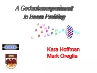
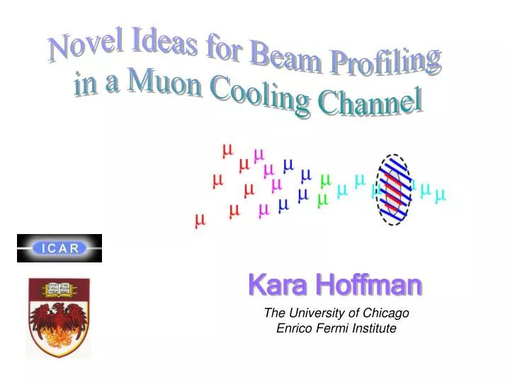
Novel Ideas for Beam Profiling in a Muon Cooling Channel. Kara Hoffman. The University of Chicago Enrico Fermi Institute. The challenge. While disturbing the beam as little as possible measure: intensity size/profile (in 2 dimensions?) timing between bunches or pulses

E N D
Novel Ideas for Beam Profiling in a Muon Cooling Channel Kara Hoffman The University of Chicago Enrico Fermi Institute
The challenge • While disturbing the beam as little as possible measure: • intensity • size/profile (in 2 dimensions?) • timing between bunches or pulses • The detection medium must be radiation hard. • The beam must be accurately measured in an environment with a lot of noise from rf cavities, etc. • The profiler and associated readout/power cables must fit within the design of the cooling channel. • Muons are difficult to detect.
Nickel “bolometer” Carbon (actually a commercially made thin film nickel thermometer) 0.8 V 0.8 V 10 ms 20 ms Bolometry: proof it works cryostat filter lenses Xe flashlamp electronics (“homemade” from graphite foil or colloidal carbon) Signal or background? Look for thermal dependence (i.e. change in signal size, time constant). Polarity: carbon’s electrical resistivity increases with temperature while nickel’s decreases. @20K
Beamtests at ANL: setup • copper block with 1/8” hole used to mask off beam and shield the thermometer • Pulses nominally 10 nA in duration--we tried to reduce inductive noise by elongating pulses to lower instantaneous current cryostat bolometric film • /pulse • 840 nA @ 30 Hz temperature controller beampipe LH2 tank vacuum pump
Beamtests at ANL: results **It is difficult to separate inductive noise from a real thermometric signal.** • Possible remedies: • Use electronic filters to distinguish signal since thermal time constant should be much longer than the noise. • Use two bolometric materials with opposite thermal response to subtract the noise. • Use a material with a much larger thermal response. (i.e. a superconducting edge thermometer) @T=20K RESULTS INCONCLUSIVE
0.30 - 0.35 K 0.25 - 0.30 0.20 - 0.25 0.15 - 0.20 0.10 - 0.15 0.05 - 0.10 0.00 - 0.05 2s beam radius Signal expectation: the linac test facility Platinum TCR curve Corresponding % resistivity change in bolometer strip GEANT3 simulation
Bolometry findings • Advantages: • doesn’t disturb the beam • relatively inexpensive • robust • Drawbacks: • must be applied to absorber window for heat sinking – could be an issue mechanically/safetywise and cannot be removed or replaced • small signal, particularly for more diffuse beams • metal strips provide challenge in large electromagnetic noise environment • large thermal time constants do not allow for measurement of timing information Evolution of window design has produced thinner prototypes
Diamond is prized for more than just its sparkle (high refractive index)… low leakage I very fast readout no p-n junction needed low capacitance no cooling hard rad hard, strong insensitive to g’s l>220nm Makes a great particle detector! The RD42 collaboration (CERN) has been developing diamond (primarily) as a microvertex detector.
Anatomy of a diamond substrate microstrip detector… IDEA #2 Ionizing radiation (36 e-h pairs per mm per mip) sputtered metal strips/pixels (400 angstroms of titanium or chromium coated with 4000 angstroms of gold) E (>1 V/mm) diamond substrate ~500 mm thick (when used as a microvertex detector) - + - + - + - + solid electrode Essentially a very compact solid-state ionization chamber.
Diamond as a beam profiler? Diamond has not yet been realized as a microvertex detector because the signal size is small compared with silicon and single particle detection efficiency is required. However, single particle efficiency is NOT required for a beam profiler. • sensitive (2 coordinate?) measurement • fast (subnanosecond ~40ps) intrinsic response might allow temporal beam profiling, in addition to current and position measurements • free standing-accessible • low Z- very little beam loss • has been demonstrated to be rad hard to a proton fluence of at least • relatively huge signal (too huge??)
Polycrystalline CVD Diamond induced charge: dx= distance e-holes drift apart m = carrier mobility, t = carrier lifetime growth side • Carrier lifetime effected by: • size of individual crystals-grain boundaries • in grain defects and impurities substrate side
Charge collection efficiency • Charge collection efficiency is a product of: • ud-carrier drift velocity- a function of the applied electric field up to a saturation velocity • t-carrier lifetime-a function of diamond quality-commercially available diamond improving with time tails due to carrier lifetimes
diamond membrane (with person peeping through) “black” diamond unpolished diamond polished high purity diamond What kind of diamond is best suited as a beam profiler? We want to minimize the signal while exploiting the timing information. • signal size could be limited by decreasing the electric field • this approach is destructive to timing information • diamond with short carrier lifetime • small t gives faster response at the expense of efficiency • much cheaper • as thin as possible • less charge produced per mip • voltage required for maximum carrier velocity is proportional to thickness • easier to dissipate heat • diamond “membranes” can be made 1mm thick
Detector fabrication: sputtering electrodes • We have fabricated our first prototype from a piece of 500mm x 11mm x 11mm detector grade CVD diamond that was manufactured by DeBeers. • Leads were sputtered at OSU using a shadow mask—finer segmentation could be achieved with a lithographic mask.
Towards a diamond testing program… • R&D areas: • Application specific material will need to be developed, along with fast electronics. • Over what range of intensity measurements could diamond be useful? (space charge effects?) • How radiation hard is it? • Near term plans: • We are in the process of obtaining some diamond with shorter carrier lifetimes. • We plan to study the behavior of our prototype in a beam test at Argonne this summer.
Final Thoughts • Two novel concepts for beam profiling are being studied/developed at the University of Chicago. The signal to background ratio for bolometry may be too low for use in a muon cooling channel or test facility. • If CVD diamond is demonstrated as a viable beam profiling medium, it may find applications outside of the muon collaboration. • The Fermilab beams division has shown a keen interest in the outcome of CVD diamond beam tests and has offered supplies as well as technical support. • The first prototype diamond profiler has been fabricated and a beam test is being planned for the summer.