Download
1 / 17
170 likes | 176 Views
Learn about the design flow for implementing VLSI projects using FPGA, including design considerations, functional simulation, HDL synthesis, design implementation, device programming, and HDL design flow.

E N D
VLSI II 9o εξάμηνο Ηλεκτρονικός ΚύκλοςΕργαστήριοστα FPGA
FPGA Πίνακας από επανα-προγραμματιζόμενα Block (CLBs) τα οποία μπορούν να υλοποιήσουν συνδυαστική ή ακολουθιακή λογική Προγραμματισμός των CLBs και των διασυνδέσεων
Πλεονεκτήματα FPGA • Επανα-προγραμματισμός της ίδιας συσκευής • Προσομοίωση του κυκλώματος • Παραγωγή σε σύντομο χρονικό διάστημα • Σχεδιασμός του κυκλώματος σε σχηματικό διάγραμμα και HDL • Χαμηλό κόστος παραγωγής
Design Ideas Detailed Design Functional Simulation Device Programming Timing Simulation Synthesis & Implementation FPGA CPLD tpd=22.1ns fmax=47.1MHz Design Flow
Design Ideas • What are the main design considerations? • Design feasibility? • Design spec? • Cost? • FPGA/CPLD or ASIC? • Which FPGA/CPLD vendor? • Which device family? • Development time?
Detailed Design • Choose the design entry method • Schematic • Gate level design • Intuitive & easy to debug • HDL (Hardware Description Language), e.g. Verilog & VHDL • Descriptive & portable • Easy to modify • Mixed HDL & schematic • Manage the design hierarchy • Design partitioning • Chip partitioning • Logic partitioning • Use vendor-supplied libraries or parameterized libraries to reduce design time • Create & manage user-created libraries (circuits)
Functional Simulation • Preparation for simulation • Generate simulation patterns • Waveform entry • HDL testbench • Generate simulation netlist • Functional simulation • To verify the functionality of your design only • Simulation results • Waveform display • Text output • Challenge • Sufficient & efficient test patterns
assign z=a&b a z b HDL Synthesis • Synthesis = Translation + Optimization • Translate HDL design files into gate-level netlist • Optimize according to your design constraints • Area constraints • Timing constraints • Power constraints • ... • Main challenges • Learn synthesizable coding style • Write correct & synthesizable HDL design files • Specify reasonable design constraints • Use HDL synthesis tool efficiently
a z b FPGA CPLD 01011... Design Implementation • Implementation flow • Netlist merging, flattening, data base building • Design rule checking • Logic optimization • Block mapping & placement • Net routing • Configuration bitstream generation • Implementation results • Design error or warnings • Device utilization • Timing reports • Challenge • How to reach high performance & high utilization implementation?
FPGA CPLD Device Programming • Choose the appropriate configuration scheme • SRAM-based FPGA/CPLD devices • Downloading the bitstream via a download cable • Programming onto a non-volatile memory device & attaching it on the circuit board • OTP, EPROM, EEPROM or Flash-based FPGA/CPLD devices • Using hardware programmer • ISP • Finish the board design • Program the device • Challenge • Board design • System considerations
HDL Design Flow • Why HDL? • Can express digital systems in behavior or structure domain, shortening the design time • Can support all level of abstraction, including algorithm, RTL, gate and switch level • Both VHDL & Verilog are formal hardware description languages, thus portable • Typical HDL design flow • Use VHDL or Verilog to express digital systems • VHDL or Verilog simulation tool is required to simulate your project • Use high-level synthesis tool to obtain structural level design • Then use FPGA placement & routing tools to obtain physical FPGA netlist
Τι θα κάνουμε • Περιγραφή κυκλώματος σε VHDL • VHDL functional simulation • Έλεγχος των σημάτων εξόδου • Σύνθεση του κυκλώματος σε FPGA αρχιτεκτονική της Xilinx με το πακέτο Leonardo Spectrum (Exemplar)
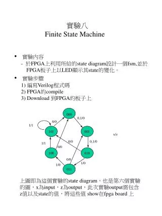
Περιγραφή σε VHDL library IEEE; use IEEE.STD_LOGIC_1164.all; entity converter is port ( i3, i2, i1, i0: in STD_LOGIC; a, b, c, d, e, f, g: out STD_LOGIC); end converter; architecture case_description of converter is begin P1: process(i3, i2, i1, i0) variable tmp_in: STD_LOGIC_VECTOR(3 downto 0); begin tmp_in := i3 & i2 & i1 & i0; case tmp_in is when "0000" => (a,b,c,d,e,f,g) <= STD_LOGIC_VECTOR'("1111110"); when "0001" => (a,b,c,d,e,f,g) <= STD_LOGIC_VECTOR'("1100000"); when "0010" => (a,b,c,d,e,f,g) <= STD_LOGIC_VECTOR'("1011011"); when "0011" => (a,b,c,d,e,f,g) <= STD_LOGIC_VECTOR'("1110011"); when "0100" => (a,b,c,d,e,f,g) <= STD_LOGIC_VECTOR'("1100101"); when "0101" => (a,b,c,d,e,f,g) <= STD_LOGIC_VECTOR'("0110111"); when "0110" => (a,b,c,d,e,f,g) <= STD_LOGIC_VECTOR'("0111111"); when "0111" => (a,b,c,d,e,f,g) <= STD_LOGIC_VECTOR'("1100010"); when "1000" => (a,b,c,d,e,f,g) <= STD_LOGIC_VECTOR'("1111111"); when "1001" => (a,b,c,d,e,f,g) <= STD_LOGIC_VECTOR'("1110111"); when "1010" => (a,b,c,d,e,f,g) <= STD_LOGIC_VECTOR'("1101111"); when "1011" => (a,b,c,d,e,f,g) <= STD_LOGIC_VECTOR'("0111101"); when "1100" => (a,b,c,d,e,f,g) <= STD_LOGIC_VECTOR'("0011110"); when "1101" => (a,b,c,d,e,f,g) <= STD_LOGIC_VECTOR'("1111001"); when "1110" => (a,b,c,d,e,f,g) <= STD_LOGIC_VECTOR'("0011111"); when "1111" => (a,b,c,d,e,f,g) <= STD_LOGIC_VECTOR'("0001111"); when others => (a,b,c,d,e,f,g) <= STD_LOGIC_vector'("0000000"); end case; end process P1; end case_description;
Ακολουθίες Ελέγχου VHDL • Ανάθεση διαφόρων τιμών στις εισόδους σε διάφορες χρονικές περιόδους • Έλεγχος αν τα αποτελέσματα είναι σωστά
Προγραμματισμός του FPGA module count8(clock, clear, enable, cout); input clock, clear, enable; output [7:0] cout; reg [7:0] cout; always @(posedge clear or posedge clock) begin if (clear == 1) cout = 0; else if (enable == 1) cout = cout + 1; end endmodule...
download cable FPGA CPLDs Programmer Προγραμματισμός