Download
1 / 8
110 likes | 377 Views
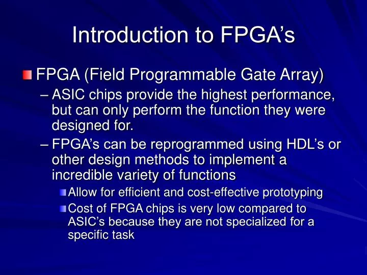
Introduction to FPGA’s. FPGA (Field Programmable Gate Array) ASIC chips provide the highest performance, but can only perform the function they were designed for. FPGA’s can be reprogrammed using HDL’s or other design methods to implement a incredible variety of functions

E N D
Introduction to FPGA’s • FPGA (Field Programmable Gate Array) • ASIC chips provide the highest performance, but can only perform the function they were designed for. • FPGA’s can be reprogrammed using HDL’s or other design methods to implement a incredible variety of functions • Allow for efficient and cost-effective prototyping • Cost of FPGA chips is very low compared to ASIC’s because they are not specialized for a specific task
FPGA: Configurable Logic Blocks • Essential FPGA component • Each CLB can be reprogrammed to implement a basic sequential or combinational circuit • Create array of CLB’s • At intersection of wires are switches • Form switching matrix
FPGA: Configurable Logic Blocks • Two 16x1 RAM blocks • 8x1 RAM block • 2 Edge-triggered D flip-flops • Multiplexers used to configure interconnects • Newer FPGA’s provide other additional hardware features
FPGA: Configurable Logic Blocks • RAM blocks act as Look Up Tables • Used to implement combinational functions • By using all 3 LUT’s, can implement any Boolean function of 5 variables
FPGA: Switching Network • PSM: programmable switching matrix configured to connect vertical and horizontal wires • Singles: connect adjacent PSMs • Doubles: connect every other PSM (traverses 2 CLBs) • Quad: traverses 4 CLBs • Global: run entire length of chip. Use tristate buffers and can be used as buses shared by several CLBs • Purpose: allows signals to be routed through fewer switching points • Global nets: low-skew signal network for high fan-out signals (clocks and reset signals)
XILINX FPGA comparison Source: www.xilinx.com
Reference(s) • Introductory VHDL From Simulation to Synthesis, Sudhakar Yalamanchili, Prentice-Hall, Inc., 2001.