Download
1 / 19
360 likes | 1.69k Views
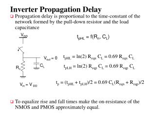
Inverter Propagation Delay. Propagation delay is proportional to the time-constant of the network formed by the pull-down resistor and the load capacitance t pHL = ln(2) R eqn C L = 0.69 R eqn C L

E N D
Inverter Propagation Delay • Propagation delay is proportional to the time-constant of the network formed by the pull-down resistor and the load capacitance tpHL = ln(2) Reqn CL = 0.69 Reqn CL tpLH = ln(2) Reqp CL = 0.69 Reqp CL tp = (tpHL + tpLH)/2 = 0.69 CL(Reqn + Reqp)/2 • To equalize rise and fall times make the on-resistance of the NMOS and PMOS approximately equal. VDD tpHL = f(Rn, CL) Vout = 0 CL Rn Vin = V DD
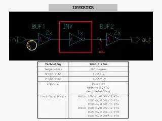
tf tr tpHL tpLH Inverter Transient Response VDD=2.5V 0.25m W/Ln = 1.5 W/Lp = 4.5 Reqn= 13 k ( 1.5) Reqp= 31 k ( 4.5) Vin Vout (V) tpHL = 36 psec tpLH = 29 psec so tp = 32.5 psec x 10-10 t (sec) From simulation: tpHL = 39.9 psec and tpLH = 31.7 psec
Inverter Propagation Delay, Revisited • To see how a designer can optimize the delay of a gate have to expand the Req in the delay equation tp(normalized) tpHL = 0.69 Reqn CL = 0.69 (3/4 (CL VDD)/IDSATn ) 0.52 CL/ (W/Ln k’n VDSATn ) VDD (V)
Design for Performance • Reduce CL • internal diffusion capacitance of the gate itself • keep the drain diffusion as small as possible • interconnect capacitance • fanout • Increase W/L ratio of the transistor • the most powerful and effective performance optimization tool in the hands of the designer • watch out for self-loading! – when the intrinsic capacitance dominates the extrinsic load • Increase VDD • can trade-off energy for performance • increasing VDD above a certain level yields only very minimal improvements • reliability concerns enforce a firm upper bound on VDD
NMOS/PMOS Ratio • If speed is the only concern, reduce the width of the PMOS device! • widening the PMOS degrades the tpHL due to larger parasitic capacitance = (W/Lp)/(W/Ln) r = Reqp/Reqn (resistance ratio of identically-sized PMOS and NMOS) opt = r when wiring capacitance is negligible • So far have sized the PMOS and NMOS so that the Req’s match (ratio of 3 to 3.5) • symmetrical VTC • equal high-to-low and low-to-high propagation delays
PMOS/NMOS Ratio Effects x 10-11 tpLH tpHL of 2.4 (= 31 k/13 k) gives symmetrical response of 1.6 to 1.9 gives optimal performance tp tp(sec) = (W/Lp)/(W/Ln)
Device Sizing for Performance • Divide capacitive load, CL, into • Cint : intrinsic - diffusion and Miller effect • Cext : extrinsic - wiring and fanout tp = 0.69 Req Cint (1 + Cext/Cint) = tp0 (1 + Cext/Cint) • where tp0 = 0.69 Req Cint is the intrinsic (unloaded) delay of the gate • Widening both PMOS and NMOS by a factor S reduces Req by an identical factor (Req = Rref/S), but raises the intrinsic capacitance by the same factor (Cint = SCiref) tp = 0.69 Rref Ciref (1 + Cext/(SCiref)) = tp0(1 + Cext/(SCiref)) • tp0 is independent of the sizing of the gate; with no load the drive of the gate is totally offset by the increased capacitance • any S sufficiently larger than (Cext/Cint) yields the best performance gains with least area impact
self-loading effect (intrinsic capacitance dominates) Sizing Impacts on Delay The majority of the improvement is already obtained for S = 5. Sizing factors larger than 10 barely yield any extra gain (and cost significantly more area). x 10-11 for a fixed load tp(sec) S
Impact of Fanout on Delay • Extrinsic capacitance, Cext, is a function of the fanout of the gate - the larger the fanout, the larger the external load. • First determine the input loading effect of the inverter. Both Cg and Cint are proportional to the gate sizing, so Cint = Cg is independent of gate sizing and tp = tp0 (1 + Cext/ Cg) = tp0 (1 + f/) i.e., the delay of an inverter is a function of the ratio between its external load capacitance and its input gate capacitance: the effective fan-out f f = Cext/Cg
Inverter Chain • Real goal is to minimize the delay through an inverter chain the delay of the j-th inverter stage is tp,j = tp0 (1 + Cg,j+1/(Cg,j)) = tp0(1 + fj/ ) and tp = tp1 + tp2 + . . . + tpN so tp = tp,j = tp0 (1 + Cg,j+1/(Cg,j)) • If CL is given • How should the inverters be sized? • How many stages are needed to minimize the delay? In Out 1 2 N Cg,1 CL
Sizing the Inverters in the Chain • The optimum size of each inverter is the geometric mean of its neighbors – meaning that if each inverter is sized up by the same factor f wrt the preceding gate, it will have the same effective fan-out and the same delay f = CL/Cg,1 = F where F represents the overall effective fan-out of the circuit (F = CL/Cg,1) and the minimum delay through the inverter chain is tp = N tp0 (1 + ( F ) / ) • The relationship between tp and F is linear for one inverter, square root for two, etc. N N N
3 8 = 2 Example of Inverter Chain Sizing • CL/Cg,1 has to be evenly distributed over N = 3 inverters CL/Cg,1 = 8/1 f = In Out 1 f = 2 f2 = 4 Cg,1 CL = 8 Cg,1
The optimum N is found by differentiating the minimum delay expression divided by the number of stages and setting the result to 0, giving + F - ( F lnF)/N = 0 • For = 0 (ignoring self-loading) N = ln (F) and the effective-fan out becomes f = e = 2.71828 • For = 1 (the typical case) the optimum effective fan-out (tapering factor) turns out to be close to 3.6 N N Determining N: Optimal Number of Inverters • What is the optimal value for N given F (=fN) ? • if the number of stages is too large, the intrinsic delay of the stages becomes dominate • if the number of stages is too small, the effective fan-out of each stage becomes dominate
Optimum Effective Fan-Out • Choosing f larger than optimum has little effect on delay and reduces the number of stages (and area). • Common practice to use f = 4 (for = 1) • But too many stages has a substantial negative impact on delay normalized delay Fopt f
Example of Inverter (Buffer) Staging N f tp 1 64 65 2 8 18 3 4 15 4 2.8 15.3 1 Cg,1 = 1 CL = 64 Cg,1 8 1 Cg,1 = 1 CL = 64 Cg,1 4 16 1 Cg,1 = 1 CL = 64 Cg,1 2.8 8 22.6 1 Cg,1 = 1 CL = 64 Cg,1
Impact of Buffer Staging for Large CL • Impressive speed-ups with optimized cascaded inverter chain for very large capacitive loads.
Input Signal Rise/Fall Time • In reality, the input signal changes gradually (and both PMOS and NMOS conduct for a brief time). This affects the current available for charging/discharging CL and impacts propagation delay. x 10-11 tp(sec) • tp increases linearly with increasing input slope, ts, once ts > tp • ts is due to the limited driving capability of the preceding gate x 10-11 ts(sec) for a minimum-size inverter with a fan-out of a single gate
Design Challenge • A gate is never designed in isolation: its performance is affected by both the fan-out and the driving strength of the gate(s) feeding its inputs. tip = tistep + ti-1step ( 0.25) • Keep signal rise times smaller than or equal to the gate propagation delays. • good for performance • good for power consumption • Keeping rise and fall times of the signals small and of approximately equal values is one of the major challenges in high-performance designs - slope engineering.
Delay with Long Interconnects • When gates are farther apart, wire capacitance and resistance can no longer be ignored. tp = 0.69RdrCint + (0.69Rdr+0.38Rw)Cw + 0.69(Rdr+Rw)Cfan where Rdr = (Reqn + Reqp)/2 = 0.69Rdr(Cint+Cfan) + 0.69(Rdrcw+rwCfan)L + 0.38rwcwL2 (rw, cw, L) Vin Vout cint cfan • Wire delay rapidly becomes the dominate factor (due to the quadratic term) in the delay budget for longer wires.