Download
1 / 33
350 likes | 502 Views
East-West Design & Test Symposium. On-chip Measurements of Standard-Cell Propagation Delay. Sergey Churayev, Bakhyt Matkarimov , Timour Paltashev Kazakh-British Technical University. September 19, 2009. 1. Abstract. We report on implementation of random sampling methodology for on-chip

E N D
East-West Design & Test Symposium On-chip Measurements of Standard-Cell Propagation Delay Sergey Churayev, Bakhyt Matkarimov, Timour Paltashev Kazakh-British Technical University September 19, 2009
1. Abstract. We report on implementation of random sampling methodology for on-chip measurements of the pin-to-pin propagation delay of single standard cells of core library. A test chip has been implemented in 0.13μm GL130SB (130nm Logic Process) technology at Dongbu HiTek, South Korea, 2007-2008, and used to monitor up to picosecond’s timing behavior of 32 DUT’s of core library. Observed mismatch between simulated and measured parameters helps to improve and verify library cell models. Reference design: S. Maggioni, A. Veggetti, A. Bogliolo, L. Croce, “Random sampling for on-chip characterization of standard cell propagation delay”, in Proceedings of the Fourth International Symposium on Quality Electronic Design, 24-26 March 2003, pp. 41- 45. Design implemented by M. Alekseyev, S. Churayev, G. Kwon, M. Kim
1. Abstract. Measurements is base of core library development
1. Abstract. Infinite cycle of core library development IP design team Test team: High precision measurement Core library design team Quality of design ~ Accuracy of core library model
1. Abstract. Random sampling for timing parameters measurements Random sampling characterization of cell timing behavior is based on measurement of cell’s pin signals at random moments of time and statistical analysis of collected data. Let us denote the signals at the pins of cell as cell state; obviously we have finite number of cell states. When we are applying periodic input signal to the cell, in general, we may observe cell state changes, and the probability to find particular cell at the given state is proportional to the time, when cell is in this state. If we collect statistics of cell states at random moments of time we can use it to create the image of cell timing behavior • Open questions: • Impact of measurements on target device • Evaluation of quality of measurements
1. Abstract. We implemented on-chip measurement methodology and made a test chip for Dongbu’s STD cells. In this report, we re-visit the basic concept and give you the test results. Basic goal of measurement is define Delay Time in delay chain of cells Black Box (Delay line of STD-cell, I/O block, special IP-core, … etc) Input under test Output under test • Main goals of design and implementation this idea: • Test Automation without high-end test equipment. • Provide highly accurate on chip measurement method. • Easy apply not only for STD cell library but also IP core, I/O, etc …
2. Introduction. • There are three main methodologies for measurement of propagation delay inside chip: • With using external probes. • With using e-beams to observe interest signal. • With using on-chip special design solution. 1 2 Test board Reference clock generator Oscilloscope Channel1 Channel2 Test chip Test board Test chip Error of measurement is too big. Reference clock generator E-beams transmitter / receiver 3 Reference clock generator Oscilloscope Channel1 Channel2 Test board Optional correlation between error and price. Test chip Price of equipment is too high. PC
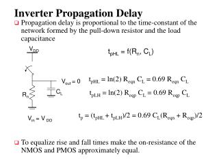
3. Main idea. T (period of clock) DUT – device under test Trr – rising time Thh Tff Tll Trr Ref. clock PAD Thh – 1 to 1 time input Tff – falling time DUT Tll – 0-0 time Output PAD output Stage in delay chain Decoder state 00 01 11 10 00 01 Random sample Depend on counter state correspond counter will increment ours value Counter Here +1 OR +1 OR +1 OR +1 CHIP
4. Schematic realization. T(00) = (N(00)*T)/N(all) L1(C1) REFCLK Input D E C O D E R Enable Counter 1 Out Clock (rising time) Fl/Fl T(rise) = (N(01)*T)/N(all) Unit under test (delay chain) Enable Counter 2 Out Clock (1 to 1 time) Key features L1(C1) = L2(C2) (!!!!!!!!!!!!) T(11) = (N(11)*T)/N(all) Enable Counter 3 Out Clock (falling time) Fl/Fl Output T(fall) = (N(10)*T)/N(all) L1(C1) XORO Enable Counter 4 Out Clock (0 to 0 time) 0.5 Standard error = (+/-) ((T(rise) * P) / N(all)) High T(all)=N00+N01+N10+N11 Enable Counter 5 Out Clock (total sample) Random ring oscillator Test chip Value of Counter 5 must be equal sum of value Counter 1, Counter 2, Counter 3, Counter 4, at the end of measurement process of test chip. It equability will be define absent of violation in clock tree.
5. Waveform. IN OUT DECODER STATE 01 11 10 00 01 11 10 00 01 11 10 00 01 11 10 00 01 11 10 00 01 11 10 00 01 11 10 00 RND RO Counter 1 00 01 02 03 Counter 2 01 02 03 04 Counter 3 02 03 04 00 01 00 01 02 03 04 Counter 4 After long time of measurement, each counter will be accumulate value, which be in proportion for time delay for each stage in delay chain. Based on this value we can easy calculate realistic time of delay inside each elements. Phase of RND RO will have random process of behavior all time, so each posedge of signal can by apply to any area, as small as possible.
6. Accuracy of measurements Calculation of delay time in delay chain (only for non inverter elements): Counter 1 T / N (1) T rising = Counter 1 + Counter 2 + Counter 3 + Counter 4 N – amount of elements in delay chain (*optional) Counter 2 (2) T / N T high = Counter 1 + Counter 2 + Counter 3 + Counter 4 T – reference period Counter3 T / N (3) T falling = Counter 1 + Counter 2 + Counter 3 + Counter 4 Counter4 T / N (4) T low = Counter 1 + Counter 2 + Counter 3 + Counter 4
6. Accuracy of measurements Calculation of delay time in delay chain (only for inverter elements): Reference clock in Trr Tff Out from delay chain (200 elements) Δ Tr Δ Tf Tr+1 Tf+1 Out from delay chain (200 elements + 1inverter) Δ Tr and Δ Tf – rising and falling time repetitively in 1 element. Δ Tr = Tr+1 - Trr Δ Tf = Tf+1 - Tff
6. Accuracy of measurements Accuracy estimation and choice period of T: Standard deviation for 1 sample For T >> T rising T rising T rising T rising σ σ (5) ~ (6) X = X = 1 T T T Standard deviation (average for N samples) σ X σ (7) = N Standard error (with combine (1), (6), (7) formulas together) T T rising T rising 1 (8) ~ σ T = = N T N
6. Accuracy of measurements Error calculation for AD2D4 delay chain: T rising of element = 100 ns T (period) = 200 ns N (Total amount of sample) = 4294967295 According formula (3) obtain average standard deviation of Trising = ± 2.1 ps. In general, the input time period T does not impact the measured propagation delay. In fact, equation (1) expresses Trr, as the product between T and the ratio Counter1/(Counter1+2+3+4), that is inversely proportional to T. However, the value of T does affect the accuracy of the measure. But with estimation formula (8) we obtain - choosing a time period T much larger that the propagation delay of interest leads to a standard error that grows with the square root of T. The best choice for period T is the minimum value that guarantees that the distance between rising and falling input transitions is safely greater than the propagation delays under measure. Error calculation for NID4 delay chain: T rising of element = 60 ns T (period) = 200 ns N (Total amount of sample) = 4294967295 According formula (3) obtain average standard deviation of Trising = ± 1.6 ps. T1<T2 T1 - bad T2 - good Error calculation for IVTD4 delay chain: T rising of element = 150 ns T (period) = 200 ns N (Total amount of sample) = 4294967295 According formula (3) obtain average standard deviation of Trising = ± 2.64 ps. Trr1 Tff1 Trr2 Tff2 T1<T2, Trr1=Trr2 and Tff1=Tff2 - constant
7. Key features of implementation. • There are two main implementation issues that may affect the accuracy of the delay measures provided by our approach: • Same condition between input and output point of delay chain. • Same condition between Flip-flop output point and input of decoder. • Matching and synchronization of the S/H circuits (Flip-Flop) used for sampling of signal and counters. • Generation of random sampling pulses independent from input waveform Vin. Test chip Module REFERENCE CLK in S/H elements Decoder Input driver Mux Counters o1 Fl/Fl Unit under test (delay chain) Key featuresL1(C1) = L2(C2) L (C) = L(C) o2 Fl/Fl Output driver OUT
7. Placement To reduce possible mismatch in synchronization of F/F circuits, we applied special constraints in the synthesis and layout design processes. Main target to be achieved is equal propagation delay from random generator to F/F elements. We used a special command script file for synthesis in Synopsys tool, and we checked synthesis results by Verilog netlist simulations. Layout of critical elements and wires was done manually. Finally, we carried out post layout SPICE simulations.
Ring oscillator 1 (17 inverters) Ring oscillator 2 (19 inverters) + Ring oscillator 238 (255 inverters) RND CLK Internal reference generator CLK FLIP FLOP 7. Random generator
8. Sequence quality estimation of random generator. For quality of RND generator we suggest to use next solution: RND RO1 (on-chip) Enable FLIP-FLOP element COUNTER for 1 N1 RND RO2 (on-chip) Or external reference generator COUNTER for 0 N0 CLK Pn1 = N1/(N1+N0) ≈ 0.5 Pn0 = N0/(N1+N0) ≈ 0.5 Probability of N(1,0) “1” much more than “0” 1 RND problem! 0.75 0.5 RND OK. TIME Time of measurements
8. Sequence quality estimation of random generator. Easy estimation of on-chip RND test generation with using Lab View system: 1. Prepare schematic: PC LABVIEW COUNTER for 1 RND out N1 TEST CHIP FLIP-FLOP element COUNTER for 0 N0 External reference generator (10 MHz) CLK 2. Build graphics with using following formulas: ≈ Probability of N(1,0) Pn1 = N1/(N1+N0) ≈ 0.5 Pn0 = N0/(N1+N0) ≈ 0.5 1 RND quality estimation 0.5 TIME Time of measurements
9. Methodology of measurement. Basic conception: Main idea consist in sequential changing the frequency of reference generator for each delay chain, with goal to minimize dummy area – make it as less as possible. This will decrease standard deviation of measurement. REFERENCE FREQUENCY GENERATOR Step 1: set REFCLK = 10 MHz REFERENCE FREQUENCY GENERATOR Step 2: set REFCLK = 20 MHz Unit under test (delay chain) Unit under test (delay chain) Useful zone (define rising & falling delay time) Useful zone (define rising & falling delay time) Dummy zone (better correlation) Dummy zone (Very large) Sequentially increase reference clock frequency, until the moment, when dummy area become as small as possible. Using special algorithms and test chip modules it was carried out automatically.
10. Test data estimation. Test condition: Reference clock= 5MHz Difference between simulation and test results explained by difference in time of simulation on workstation and on-chip measurements of test chip. Simulation time can’t cover all necessary time for calculation of delay time, it’s too big and speed of workstation is too slow for that. So: 1. Simulation time: Tsim = 0000_199Dh. 2. Real time for test: Treal = FFFF_FFFF. Tsim << Treal, so error between simulation result and test resultcan be big.
11. Interface of test chip. Test board Lab View, FPGA, PC, Etc… Test chip RESET Delay chain REF CLOCK Ref clock out Chip select BONUS PIN (optional - reserve) [09:00] Write Module of measurement AD [31:00] More simple interface will provide: 1. Easy test of chip. 2. Compatibility between old and new version of test chip (Not necessary make new board and program for capture data). 3. Flexible address module allocation for each delay chain. DATA [31:00] UART IN UART module UART OUT
11. Interface of test chip. • To get easy access for each module of test chip, we must design special design agreements for interface of test chip. It will let in future design new test chip without change of test board and communication program. • New interface must include next pin (total available 144 pin) : • RESET : 1 pin • Ref clock : 1 pin • Chip select : 1 pin • WRITE : 1 pin • ADDRES : 31 down to 0 pins • DATA : 31 down to 0 pins • Ref clock out : 1 pin • Uart in : 1 pin • Uart out : 1 pin • Bonus pin : 10 pins • Power pins : 63 pins • TOTAL in use : 144 pins (81 user pins + 63 power pins (VCC+GND))
11. Interface of test chip. Memory address allocation for new test chip * Because each measurement module have 4 counter, we should use each 4 address for 1 measurement module.
12. Conclusion. We have presented an approach of on-chip delay measures based on random sampling. The proposed approach is independent of the nature of the DUT, making it suitable for measuring the propagation delay of any combinational path across a single cell, a complex combinational unit, or a single interconnect. The distinguishing feature of our technique is the capability of measuring single-cell delays, thus enabling the characterization of corner cases, without using high-performance test equipments. Moreover, the compact implementation enables the integration of many DUTs on the same die. A prototype test chip with an array of 32 DUTs has been realized in GL130SB (130nm Logic Process) technology.
12. Conclusion. • Bonuses of using this idea: • Measurement of Single DUT propagation delay • Distinguish between raising and falling propagation delay’s • Measurement equipments can be placed as close as possible to the test structure, thus improving the signal to noise ratio. • Delay measures can be performed in the actual operating conditions. • Many test structures can be integrated on the same die. • A large number of measures can be simultaneously performed. • Only low-cost external instrumentation is required. • Minus: • Random sampling method for on-chip characterization require high accuracy in chip design. • Time of simulation & test is too big. In real case is high probability, that external & internal condition will influent on schematic than more, than more test time. To decrease simulation and test time need apply special algorithms of calculation middle value of test. • For achieved more accuracy result we need to improve design special module of observation & control, to decrease dummy zone of measurement (1 - > 1 & 0 - > 0) with using external (internal) reference clock.
13. References. • O. Coudert, “Timing and design closure in physical design flows,” in Proceedings of ISQED pp. 511-516, 2002. • J. A. Davis, et al. "Interconnect Limits on Gigascale Integration (GSI) in the 21st Century," in Proceeding of IEEE vol. 89, no. 3, pp. 305- 324, 2001. • B. E. Stine, E. Chang, D. S. Boning, and J. E. Chung, “Analysis and decomposition of spatial variation in integrated circuit processes and devices,” in IEEE Transactiona on Semiconductor Manufacture, vol. 10, pp.24-41, 1997. • W. H. Kao, Chi-Yuan Lo, M. Basel, and R. Singh, “Parasitic extraction: current state of the art and future trends,” Proceeding of IEEE, vol. 89, no. 5, pp. 729-739, 2001. • S. Maggioni, A. Veggetti, A. Bogliolo, L. Croce, “Random sampling for on-chip characterization of standard cell propagation delay”, in Proceedings of the Fourth International Symposium on Quality Electronic Design, 24-26 March 2003, pp. 41- 45. • S. K. Thompson, Sampling, 2nd Edition, Wiley, 2002.
P1. Ring oscillators module analyzing. Test chip Ring oscillator 1 Ring oscillator 2 • Same condition: • Schematic. • Layout. • Process variation. • Noise. • Temperature. • Etc… 1024 IVD4 elements 1024 IVD4 elements IVD4 delay time = T/1024 Ideal case for simulation Simulation RO 1 Simulation RO 2 Phase error depend on: Δθ= f (1,2,3,4,5,6…) Current ideal case: Θn = Θn-1 ±Δθ = const = 0
P1. Ring oscillators module analyzing. Net list + SDF simulation result : Θn = Θn-1 ±(Δθerror layout ≠0); Fro1 ≈ Fro2; NET+SDF RO 1 NET+SDF RO 2 • Layout is not same for NET + SDF simulation. • Tro1 = 51696 ps => Fro1 = 19343856 Hz. • Tro2 = 51034 ps => Fro2 = 19594779 Hz. Δθerror layout ≈ 662 ps Δθ(2,3,4,5,6) ≈ RND ps Real silicon simulation result : Θn = Θn-1 ±Δθerror layout ±Δθerror (1,3,4,5,6) IVD4 delay ≈ 50 ps Real RO 1 Real RO 2 Δθerror layout Δθerror (2,3,4,5,6)
P2. Phase error accumulation methodology. The main idea consist in start both ring oscillator at same time and stop when value counter 2 not will be equal value counter 1. To define this state we use comparator. Each enable signal of counter connect to the comparator output. Because ring oscillator have different amount of elements – after some time counter value1 and counter value 2 became not equal, and comparator will produce stop condition for counter1,2,3. Counter 3 calculate time after start. With using value of counter3 we can obtain total time between start and stop point and define propagation delay time in 2 last elements. Ring oscillator1 (odd elements) Clock Counter 2 Out Enable Enable Start / stop Comparator REFCLK Synchronizer DATA multiplexer Enable Counter 1 Out clock Enable Counter 3 Out clock Enable Ring oscillator2 (odd elements + 1)
P2. Phase error accumulation methodology. θerr=0 (start) θerr=0 (stop) Θn = Θn-1 ± (Δθelement ≠0) Θn = Θn-1 ± (Δθelement ≠0); P - period Reference clock RO1 RO2 Start/stop Counter 1 01 02 03 04 … 2000 Counter 2 … 1001 03 01 02 04 Counter 3 01 02 03 04 … 1000 Stop of the measurement T (time of measurement) = P * Ncounter3 Delay time = T / 2*(Ncounter2-1) Delay time = T / 2*Ncounter3
P2. Phase error accumulation methodology. For example : P – period = 10 ns. ΔD – delay in 1 element = 10 ns Ring oscillator 2 = 10 elements. Ring oscillator 3 = 11 elements. After finished calculation – ΔD = T simulation / 2*N3= (P * Value counter1) /2*Value_counter3 = 10 ns Stop condition Next cycle of iteration