Download
1 / 39
390 likes | 496 Views
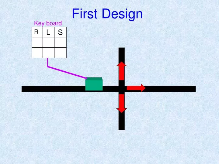
First Design. Key board. R. L. S. Second Design. B. A. Third Design. Key board. B. C. D. B. A. D. C. 1. 1. 0. 1. 2. 3. 1. 0. 1. 4. 5. 6. 0. 1. 1. 7. 8. 9. 1. 1. 1. 1. 1. 1. 1. 0. 1. Microcontroller 8051. Contents:. Introduction

E N D
First Design Key board R L S
Second Design B A
Third Design Key board B C D B A D C
1 1 0 1 2 3 1 0 1 4 5 6 0 1 1 7 8 9 1 1 1 1 1 1 1 0 1
Microcontroller 8051
Contents: • Introduction • Block Diagram and Pin Description of the 8051 • Registers • Memory mapping in 8051 • Stack in the 8051 • I/O Port Programming • Timer • Interrupt
Why do we need to learn Microprocessors/controllers? • The microprocessor is the core of computer systems. • Nowadays many communication, digital entertainment, portable devices, are controlled by them. • A designer should know what types of components he needs, ways to reduce production costs and product reliable.
Different aspects of a microprocessor/controller Hardware :Interface to the real world Software :order how to deal with inputs
The necessary tools for a microprocessor/controller • CPU: Central Processing Unit • I/O: Input /Output • Bus: Address bus & Data bus • Memory: RAM & ROM • Timer • Interrupt • Serial Port • Parallel Port
CPU for Computers No RAM, ROM, I/O on CPU chip itself Example:Intel’s x86, Motorola’s 680x0 Microprocessors: General-purpose microprocessor Many chips on mother’s board Data Bus CPU General-Purpose Micro-processor Serial COM Port I/O Port RAM ROM Timer Address Bus General-Purpose Microprocessor System
Microcontroller : • A smaller computer • On-chip RAM, ROM, I/O ports... • Example:Motorola’s 6811, Intel’s 8051, Zilog’s Z8 and PIC 16X CPU RAM ROM A single chip Serial COM Port I/O Port Timer Microcontroller
Microprocessor vs. Microcontroller • Microcontroller • CPU, RAM, ROM, I/O and timer are all on a single chip • fix amount of on-chip ROM, RAM, I/O ports • for applications in which cost, power and space are critical • single-purpose Microprocessor • CPU is stand-alone, RAM, ROM, I/O, timer are separate • designer can decide on the amount of ROM, RAM and I/O ports. • expansive • versatility • general-purpose
Block Diagram External interrupts On-chip ROM for program code Timer/Counter Interrupt Control Timer 1 On-chip RAM Counter Inputs Timer 0 CPU Serial Port Bus Control 4 I/O Ports OSC P0 P1 P2 P3 TxD RxD Address/Data
Vcc P1.0 1 40 P0.0(AD0) P1.1 2 39 P0.1(AD1) P1.2 3 38 P0.2(AD2) P1.3 4 37 8051 (8031) P0.3(AD3) P1.4 5 36 P0.4(AD4) P1.5 6 35 P0.5(AD5) P1.6 7 34 P0.6(AD6) P1.7 8 33 P0.7(AD7) RST 9 32 (RXD)P3.0 EA/VPP 10 31 (TXD)P3.1 ALE/PROG 11 30 PSEN (INT0)P3.2 12 29 P2.7(A15) 13 28 (INT1)P3.3 (T0)P3.4 P2.6(A14) 14 27 (T1)P3.5 P2.5(A13) 15 26 P2.4(A12) (WR)P3.6 16 25 P2.3(A11) (RD)P3.7 17 24 P2.2(A10) XTAL2 18 23 P2.1(A9) XTAL1 19 22 P2.0(A8) GND 20 21 Pin Description of the 8051
Figure (b). Power-On RESET Circuit Vcc + 10 uF 31 EA/VPP X1 30 pF 19 11.0592 MHz 8.2 K X2 18 30pF RST 9
Vcc 10 K Port 0 P0.0 P0.1 DS5000 8751 8951 P0.2 P0.3 P0.4 P0.5 P0.6 P0.7 Port 0 with Pull-Up Resistors
A B R0 DPTR DPH DPL R1 R2 PC PC R3 Some 8051 16-bit Register R4 R5 R6 R7 Some 8-bitt Registers ofthe 8051 Registers
7FH Scratch pad RAM 30H 2FH Bit-Addressable RAM 20H 1FH Register Bank 3 18H 17H Register Bank 2 10H 0FH (Stack) Register Bank 1 08H 07H Register Bank 0 00H Stack in the 8051 • The register used to access the stack is called SP (stack pointer) register. • The stack pointer in the 8051 is only 8 bits wide, which means that it can take value 00 to FFH. When 8051 powered up, the SP register contains value 07.
Timer: Timer : :
Numerical Bases Used in Programming • Hexadecimal • Binary • BCD
Hexadecimal Basis • Hexadecimal Digits: 1 2 3 4 5 6 7 8 9 A B C D E F A=10 B=11 C=12 D=13 E=14 F=15
Decimal, Binary, BCD, & Hexadecimal Numbers (43)10= (0100 0011)BCD= ( 0010 1011 )2 = ( 2 B )16
Register Addressing Mode MOV Rn, A ;n=0,..,7 ADD A, Rn MOV DPL, R6 MOV DPTR, A MOV Rm, Rn
Direct Addressing Mode Although the entire of 128 bytes of RAM can be accessed using direct addressing mode, it is most often used to access RAM loc. 30 – 7FH. MOV R0, 40H MOV 56H,A MOV A, 4 ; ≡ MOV A, R4 MOV 6, 2 ; copy R2 to R6 ; MOV R6,R2 is invalid !
Immediate Addressing Mode MOV A,#65H MOV R6,#65H MOV DPTR,#2343H MOV P1,#65H
SETB bit ; bit=1 CLR bit ; bit=0 SETB C ; CY=1 SETB P0.0 ;bit 0 from port 0 =1 SETB P3.7 ;bit 7 from port 3 =1 SETB ACC.2 ;bit 2 from ACCUMULATOR =1 SETB 05 ;set high D5 of RAM loc. 20h Note: CLR instruction is as same as SETB i.e.: CLR C ;CY=0 But following instruction is only for CLR: CLR A ;A=0
DEC byte ;byte=byte-1 INC byte ;byte=byte+1 INC R7 DEC A DEC 40H ; [40]=[40]-1
LOOP and JUMP Instructions Conditional Jumps :
Call instruction SETB P0.0 . . CALL UP . . . CLR P0.0 . . RET UP: