Download
1 / 1
10 likes | 125 Views
Puneet Sharma † (sharma@ucsd.edu ) Advisor: Prof. Andrew B. Kahng ‡† Jointly with Mr. Sherief Reda ‡ † Electrical & Computer Engineering ‡ Computer Science & Engineering. On-Line Adjustable Buffering for Runtime Power Reduction ( http://vlsicad.ucsd.edu ). Introduction.

E N D
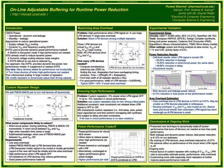
Puneet Sharma† (sharma@ucsd.edu) Advisor: Prof. Andrew B. Kahng‡† Jointly with Mr. Sherief Reda‡ †Electrical & Computer Engineering ‡Computer Science & Engineering On-Line Adjustable Buffering for Runtime Power Reduction( http://vlsicad.ucsd.edu ) Introduction Restricting Area Overhead Experimental Validation • CMOS Power: • Operational – dynamic and leakage • Standby – leakage • Approaches to reduce operational power: • Supply voltage (VDD) scaling • Dynamic VDD and frequency scaling (DVFS) • DVFS used to provide dynamic power-performance tradeoff • Switch to low-power mode if high performance not needed • VDD already small to reduce dynamic power • Dynamic voltage scaling reduces noise margins • DVFS difficult to use due to reduced VDD • Our approach, like DVFS, provides dynamic low-power, low-performance modes supplement or replace DVFS • Key idea: Many devices added for performance not functionality Turn those devices off when high-performance not needed • Poor interconnect scaling large number of repeaters • We modify repeaters to dynamically adjust their driving capacity • Problem: High performance when LPM signal on use large LPM devices large area overhead • Solution:Share LPM devices among multiple repeaters • Fewer LPM devices but • virtual VDD (V’DD) and • VSS (V’SS) need routing • Note: All LPM devices drive • V’DD and V’SS • How many LPM devices • needed? • Compute simultaneous • switching rate (SSR) by • finding the max. #repeaters that have overlapping timing windows. Time = O(RlogR) (R = #repeaters) • Find total width of all repeater devices (=WR) • For good performance, width of LPM devices = 2xSSRxWR • Typical SSR=~10% small area overhead • Experimental Setup • Circuits: s38417 (8,890 cells), AES (15,272), OpenRisc (46,732) • Tools: Synopsys HSPICE (SPICE), Design Compiler (synthesis, timing and power analysis), Cadence SoC Encounter (P&R), SignalStorm (library characterization), TSMC 90nm library models • Other settings: power and timing analysis at slow corner, VDD of 1.1V and 0.9V, activity factor of 0.01. • Power Reduction Results • Cell-level results: when LPM signal is turned ON • 20-20% reduction in leakage • 15-30% reduction in short-circuit power (for same slew) • 45-65% increase in delay • Circuit-level results: • Both dynamic and leakage power reduce • 6-12% reduction in total power at low performance modes • Area Overhead Estimation • Area overhead due to LPM devices is 0.91% to 5.57%. May be smaller as LPM devices placeable in whitespace. • Routing overhead: V’DD and V’SS nets routed as min. Steiner trees and found shorter than scanchain; LPM signal has short wirelength as #LPM devices is small. LPM devices shared by two inverters Custom Repeater Design Ensuring High Performance • We add PMOS-NMOS pair to turn half devices off dynamically • What power components likely to reduce? • Short-circuit power: During switching, PMOS & NMOS ON momentarily short circuit between VDD and VSS • High when transition time (slew) is large • Subthreshold leakage: when one of PMOS-NMOS pair between VDD and VSSON • Requirements: • Low area overhead • Added PMOS-NMOS pair (LPM devices) take area • LPM (low-power mode) signal to be routed or locally generated • Layout of the new cell must be simple and low area overhead • High performance when LPM signal OFF • On-resistance of LPM devices may reduce performance • Good power-performance trade-off • Problem: Custom repeaters ~5% slower when LPM signal OFF • Up to ~5% reduction in circuit performance Solution:use custom repeaters only on non- timing-critical paths Additional constraint: slew constraints not violated when LPM signal is OFF or ON. We characterize custom repeaters (i.e., find delay, slew, power, input capacitance) and then perform remapping with synthesis tool subject to delay and slew constraints. No loss in circuit performance & no slew violations Traditional Inverter Custom Inverter Conclusions & Ongoing Work Power-Performance Tradeoff • Presented new technique to dynamically trade-off power-performance that turns off devices not needed at less than peak performance • Both leakage and dynamic power reduce; total power reduction is 6-12% on our testcases • By sharing of LPM devices, area overhead reduced to <5.57% • No adverse affect on performance of the circuit when LPM signal is off. • Ongoing work: • Actual layout of custom repeater with routing of V’DD, V’SS, LPM nets to accurately estimate power, performance, area overhead • Customizing more cells especially clock repeaters to further improve power-performance trade-off. • Power-performance for circuit • AES shown • Utilize slack to reduce power • when high performance not • needed • Power lowered or unchanged • with LPM • Alternatively, unchanged or • higher performance given • power budget • Higher performance per watt Power-performance w/ DVFS & DVFS combined w/ LPM