Download
1 / 16
160 likes | 261 Views
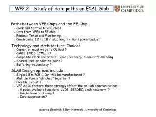
Study of 1.5m data paths along CALICE slabs. the ‘problem’ & its scale technology and architecture choices test-slab design options current status outlook and plans. Single side of a slab. ~1500mm. front-end (FE) board + chip. sensors. very front-end (VFE) chips.

E N D
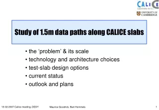
Study of 1.5m data paths along CALICE slabs the ‘problem’ & its scale technology and architecture choices test-slab design options current status outlook and plans 13-02-2007 Calice meeting, DESY
Single side of a slab ~1500mm front-end (FE) board + chip sensors very front-end (VFE) chips clock, controls, power data The ‘problem’ & its scale • Paths between VFEs and FE: • Clock and Control to VFE chips • Data from VFEs to FE chip • Readout Token and Monitoring 13-02-2007 Calice meeting, DESY
Slab design • Constraints on data paths: • Limited space (800 mum PCB thickness) • Tight power budget (~0 mW) • Long slabs (~1.6m) Technology choices: • VFE chip on board: build slab in segments to conserve yield • Introduces a joint between PCBs… • CMOS signalling where possible for low power consumption 13-02-2007 Calice meeting, DESY
Signal distro & readout architecture • Signal routing options on a panel: • common lines vs. point-to-point • Signal routing along a full slab: • slab-wide or per-panel distribution • how much redundancy should be built in ? • should clock & data be combined for increased reliability ? • Fast links at low duty cycle are power efficient • Power-speed tradeoff governed by transmission line characteristics 13-02-2007 Calice meeting, DESY
PCB traces = Transmission Lines Run ACTL simulation with following geometry: • 64 mu (2.5 thou) PCB thickness • 50 mu (2.0 thou) pre-preg thickness • 17 mu (0.7 thou) = 0.5 oz Cu layer low Z and high C makes CMOS noisy and power-hungry 13-02-2007 Calice meeting, DESY
Slab Panel PCB board build • Recent revision of Slab PCB thickness = 800um • Expected thickness ~ 770um + resist + text • Top, Bottom and Differential Signal layers • 5 Power and Ground Planes 13-02-2007 Calice meeting, DESY
Estimated data readout speed • Assumptions: • 72 channels/chip • 5k events/bx train • 1 ms train length • 5 Hz repetition rate • readout of all channels for all BX’es results in unrealistically high data rates • duty cycle/buffering reduces rate 200x • readout speed determined by data reduction through zero-suppression • ultimate case: few events/chip/Bx train (still dominated by noise…) x Gbps/chip xxx Mbps x-xxx Mbps threshold=0.5 MIP 80 e-,h+/mum Si x Mbps 13-02-2007 Calice meeting, DESY
Slab model Build a slab model to test the many variables • FPGAs instead of VFE chips • 1 FPGA mimics 2 VFE chips • HCAL in VHDL serves as VFE ~ 240mm • Many signal distro/routing options incorporated in PCB • Many output standards and speeds supported by FPGA • Includes long, folded lines for measurements on transmission lines 13-02-2007 Calice meeting, DESY
Slab model: current status Interface Card • 10 PCBs manufactured • PCB support bars for slab assembly • 1 PCB populated and powered: initial tests (JTAG chain, programming of devices) Slab segment PCB Support bar 13-02-2007 Calice meeting, DESY
Inter-Panel Bridging Pads Mounting Rail Alignment Pins Panel PCB interconnects 13-02-2007 Calice meeting, DESY
The ends of the slab • End-of-slab (FE) task: • data collection from pVFE chips • data buffering • clock distribution: 40MHz & 1MHz • control signals: reset, initialisation • JTAG programming chain • power distribution • signals for tests & measurements (BER) • communication with outside world 13-02-2007 Calice meeting, DESY
Test slab setup FE board intermediate board slab panel 0 • clock distribution • power distribution • interface with slab • clock generation • control signals (token,etc.) • data reception & buffering • interface with outside world • Digilent starter kit serves as FE board: • Xilinx Spartan 3E-500 FPGA • supports many IO standards over large speed range • large user connector (~40x I/O pins up to 100MHz) • 32MB SDRAM • Ethernet 10/100 PHY • USB-JTAG programming 13-02-2007 Calice meeting, DESY
Test slab status • Slab panels: 1 panel populated and being tested not all panels are to be equipped with FPGAs • Intermediate board: schematics, PCB design well under way • Firmware for pVFE FPGAs is ready ‘v.0.99’ • Essentials for FE firmware available clock manager, deserialiser, data buffer 13-02-2007 Calice meeting, DESY
pVFE and FE firmware: BER test • First Bit Error Rate (BER) test: • all logic in single FPGA • separated Tx/Rx blocks • signals routed through external wires The expected ‘bathtub’ plot looks a bit ragged, but it has a clear bottom –in the wrong place? 13-02-2007 Calice meeting, DESY
Test & measurement programme • BER tests on panels with multiple pVFEs • different clocking & readout schemes • other options: clock+data encoding, redundancy routing, etc. • folded traces: transmission characteristics • determine data transmission speed limits 13-02-2007 Calice meeting, DESY
Outlook & Plans • Complete test slab programme • Optimise PCB wrt the data rate requirements • Determine ultimate DAQ performance requirements using test slab PCB max. throughput figures • Contribute to the Calice slab design by providing feedback –where and if appropriate • Make our components (design & test tools) available to the Calice programme • Start design study of FE board: • possibly including a redesigned intermediate board • modular design for maximum flexibility 13-02-2007 Calice meeting, DESY