Download
1 / 79
880 likes | 1.3k Views
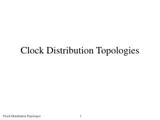
Clock Distribution. Shmuel Wimer Bar Ilan Univ. Eng. Faculty Technion, EE Faculty. clk 3. Clock Distribution. ext_clk. gclk. External Clock. Clock Generator. Buffers. Gaters. clk 2. clk 1. Clocked Elements. Chip. Clock System Architecture.

E N D
Clock Distribution Shmuel Wimer Bar Ilan Univ. Eng. Faculty Technion, EE Faculty
clk3 Clock Distribution ext_clk gclk External Clock Clock Generator Buffers Gaters clk2 clk1 Clocked Elements Chip Clock System Architecture Chip receives external clock through I/O pad. Clock generator adjusts the global clock to the external clock. Global clock is distributed across the chip. Local drivers and gaters drive the physical clocks to clocked elements.
Global Clock Generation • Receives external clock signal and produce the global clock distributed across the die. • A large skew occurs between external clock and the physical clocks at clocked elements due to delay of distribution network (wires, buffers, gaters). • Therefore, data at clocked elements is no more in sync with data at I/O pins. • Phased Locked Loop (PLL) compensates this delay. • PLL can perform frequency multiplication to obtain the required on-chip frequencies.
Chip A Chip B CLKin ext_clk ref_clk CLKout PLL clk_out Din fdbk_clk Dout Dout gclk Din clk Clock Distribution Synchronous Chip Interface with PLL Chip A communicates synchronously with chip B Chip B uses the clock sent by chip A. Data in and out must be synchronized to the common clock. A PLL produces the global clock of chip B such that it is in sync with the external clock.
Loop Filter Charge Pump I I C Up ref_clk R Voltage Controlled Oscillator clk_out Phase Detect Vctrl fdbk_clk Down M N How PLL Works?
Q_A: B should go faster 1 A D Q B CLR Q_B: B should go slower 1 CLR D Q Phase – Frequency Detector (PFD) The two flip-flops receive the signals at their clock input (one is usually a reference and the other is the sampled). The output of the leading flip-flop is 1 for the lead duration. Once the lagging signal arrives, a reset turns both Q_A and Q_B to zero.
A: reference B: sampled Q_A: sampled should go faster Q_B: sampled should go slower What happens when the reference and the sampled signals are a shift of each other? The spikes at Q_B are a result of the delay of the AND gate driving the CLR input of flip-flip and the internal delay from CLR to Q.
A: reference B: sampled Q_A: sampled should go faster Q_B: sampled should go slower What happens when the reference and the sampled signals have different frequencies? Sampled is more often 1-value than the reference is, since rising edge of B occurs more often than rising edge of A.
faster 1 Icp CLK_ref Vctrl Sup D Q Sdn CLK_fdbk Icp CLR 1 slower CLR D Q Charge Pump Converts PFD error (digital) to charge (analog), which then controls PLL VCO.
Vcc V Iin Iout N1 N2 P1 P2 Iout Iin V Vss Current Mirror Charge pump consists of current mirrors which are sources of constant current. Device N1 is in saturation since its gate is connected to high voltage. Ids (=Iin) depends only on Vgs. Vgs is similar in N2, hence Iout=Iin. This is an ideal current source with infinite output impedance since Iout is independent of N2 load; a change in output voltage doesn’t affect Iout. Current mirror works similarly for P transistors.
Vcc Vcc R load – determines the current through current mirror C I I I I I I faster R P-type current mirror Switch – open when faster = 1 Vout slower Switch – open when slower = 1 N-type current mirror How Charge Pump Works? Vss
Vcc Vcc C R faster=1 Vout slower=0 Vss Faster Mode Vout → Vcc
Vcc Vcc C R faster=0 Vout slower=1 Vss Slower Mode Vout → Vss
Vcc C R + Vctrl Vctrl - Loop Filter Differential amplifier connected as a unity-gain follower is used.
Vout Voltage Controlled Oscillator (VCO) A Ring Oscillator cascades an odd number of inverters and feeds back the last output to first inverter (even number of inverters will be stable). It starts to oscillate spontaneously. Frequency can be controlled by number of inverters and supply voltage of inverter (higher voltage obtains faster inverter).
Buffering for driving clk_out Vctrl Vcc clk_out Vss Ring of 5 inverters Level Converter from Vctrl-Vss to Vcc-Vss Components of VCO Vctrl
Delay Locked Loop (DLL) • It is a variant of PLL that uses voltage-controlled delay line rather than oscillator. • It adjust phase only. Frequency multiplication is impossible. • It is simpler than PLL, less sensitive to Vctrl noise and requires simpler loop filter. • It is very difficult to correctly design PLL and DLL. It requires expertise in control systems and analog circuit design.
Loop Filter Charge Pump I I C Up ref_clk R Voltage Controlled Delay Line clk_out Phase Detect Vctrl fdbk_clk Down How DLL Works?
In Out In Out Delay Line
clk1 clk2 clk3 clkn Tree Clock Network (Unconstrained) No constraints imposed on buffers and wires. Used mostly by automatic tools in automatic synthesis flows. Can be used for small blocks within large design. Tools aim at minimizing the variance of clock delays.
Serpentine routing or extra buffers may be introduced to obtain small variance. Constraints on power can be imposed by limiting number and size of clock buffers and width of wires.
Grid feeds flops directly, no local buffers Clock driver tree spans height of chip Internal levels shorted together Clock Distribution with Grids Low skew but high power
Clock drivers are on perimeter Clock drivers are on grid points
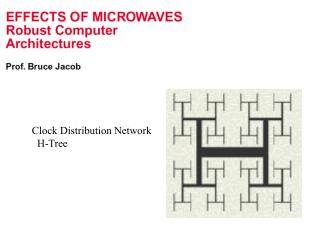
H-Tree RC-Tree Recursive pattern to distribute signals uniformly with equal delay over area Each branch is individually routed to balance RC delay Clock Distribution with Trees More skew but less power
sequential elements Clock H-Tree chip / functional block / IP clock / PLL
Delay Calculation We use Elmore delay model. Sub trees are modeled as capacitive loads
Clock Skew and Jitter • Clock should theoretically arrive simultaneously to all sequential circuits. • Practically it arrives in different times. The differences are called clock skews. • Skews result from paths mismatches, process variations and ambient conditions, resulting physical clocks. • Most system distribute a global clock and then use local clock gaters located near clocked elements. Clock skew consists of the following components:
Systematic is the portion existing under nominal conditions. It can be minimized by appropriate design. • Random is caused by process variations like devices’ channel length, oxide thickness, threshold voltage, wire thickness, width and space. It can be measured on silicon and adjusted by delay components. • Drift is caused by time-dependent environmental variations, occurring relatively slowly. Compensation of those must takes place periodically. • Jitter is rapid clock changes, occurring by power noise and clock generator jitter. It cannot be compensated.
Skew, Clock Cycle and Design Margins Clock Jitter is the same order as skew, but far more difficult to compensate.
Q Tclk1 1 2 m Clock Generator CL Tclk2 1 2 n D Skew Modeling Point of divergence
How much of the power is consumed by the far end drivers of clock tree?
Given the number of sequential elements in a block, at least 50% of the switching power is consumed by the far end drivers (clock tree is binary, k=2). This number approaches 1 rapidly with k growth. Example: Assume a block with 214 sequential elements and H-tree clock distribution. Then k=4 and m=7. The far end drivers consume nearly 75% of the clock tree switching power, while adding the next upper level drivers brings it to more than 90%.
Active Clock De-Skewing • Compensates process variability, temperature gradients, imperfect design. • Can be implemented for global fixes (small HW overhead) or local fixes (high HW overhead). • Can be used at testing for one time fix (variability occurring during manufacturing), or dynamically concurrently with chip operation. • Its implementation is a difficult design challenge.
Intel’s Pentium2 De-Skewing System 1998, 450MHz Clock 0.25u process 60pSec skew w/o fix 15pSec skew with fix Two clock spines for two clock regions. A phase detector detects relative shifts. Clock of a region is shifted by a delay line.
Delay line consists of two cascaded inverters. Each has a programmable load consists of eight parallel P-N gate capacitors. The shift register stores a thermometer code for load programming in steps of 12pSec.
PLL Intel’s IA64 Itanium1 De-Skewing System 2000, 800MHz clock 0.18u process 28pSec skew with fix X4 increase w/o fix 30 independent de-skew regions. Each cluster is driven from a global H-tree. Delay circuit in de-skew region are similar to Pentium3 with 20-bit registers.
Proposal for H-Tree Clock De-Skew – Hierarchical Approach If a phase detector (PD) has a skew guard band g, then guard bands may accumulate along tree paths. For example, if a logic stage is shared between region B and C, it may add 7g time units to path delay.
Proposal for H-Tree Clock De-Skew – Mesh Approach Clock is distributed by H-tree, but de-skew takes place by neighbor leaves phase detection. A delay buffer accepts phase inputs from its 4 neighbors and then decides of whether to increase, decrease or not change its delay.