Download
1 / 15
150 likes | 294 Views
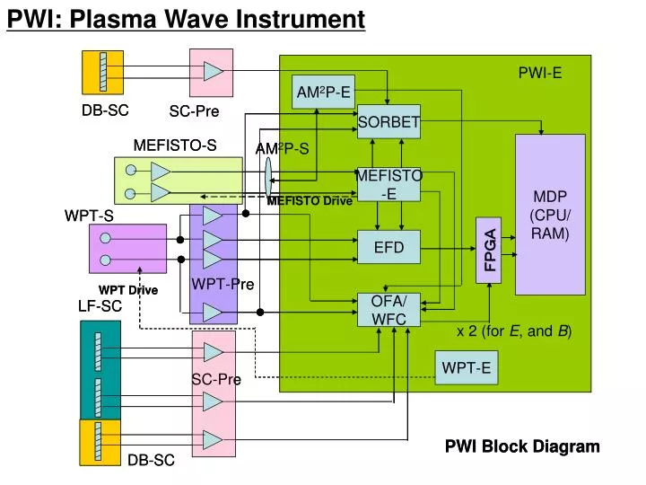
PWI: Plasma Wave Instrument. Update of the PWI status (after the previous SWG). Past major events: October 13: PWI 6th Kyoto meeting ( Kyoto Univ.) Discussion of the electrical interface and EMC October 18: EMC board meeting (ISAS) November 21: EGSE Meeting ( Meudon ) PWI Common GSE

E N D
Update of the PWI status (after the previous SWG) Past major events: October 13: PWI 6th Kyoto meeting(Kyoto Univ.) Discussion of the electrical interface and EMC October 18: EMC board meeting (ISAS) November 21:EGSE Meeting(Meudon) PWI Common GSE December 6: EMC tests of TWTA (Kanazawa)
EWO • BBM Development & Tests: • DC CAL/BIAS、Loop gain control • LPF of WFC/OFA/EFD-E & B AM2P • Power supply : • Voltage conversion- Usage of -12V ->-5V • -> increase of power consumption • Under the discussion of the size and weight • considering the additional functions • (To be discussed this week in Kanazawa)
MEFISTOupdate 22 March 2006 • Max. amplitude (LF) 500 mV/m • Bit resolution 0.015 mV/m • Spacecraft potential -100 to +100 V • Frequency range DC – 3 MHz Sensor wire, 0.1-0.3 mm 1-2 m 13-14 m TiAlN probe 40 mm diameter “puck” Boom, connected to s/c ground
Second-Surface Mirror Development Work is on-going to develop an SSM, mainly for the boom wire. Goal is to achieve: • Mechanical flexibility • Electrical conductivity, to keep all satellite surface potentials within ~1V • Temperature below 150°C to avoid damage to wire insulator material
Thermal Modelling • Thermal model of MEFISTO “stand-alone” has been developed and run • All temperatures within acceptable limits for all mission phases • Model has been supplied to JAXA, for integration with spacecraft level model • Currently model details are being discussed and iterated with JAXA thermal engineers
Electronics • Design and development of flight electronics is proceeding as planned • Co-ordinated EGSE development in Europe is progressing Mechanics • Design and development of flight machannics is proceeding as planned
Funding status • Swedish National Space Board • Royal Institute of Technology • Swedish Institute of Space Physics have signed funding commitments
Requests (reminder) • Normal sun angle > 92 deg, i.e., 93 +/- 1 deg, if possible • Maximum potential difference on external surfaces of order 1 V, i.e., all external surfaces must be (reasonably) conductive
New ASIC design (January 2006) • Analogue functions on a single chip : • Specific design (Full Custom) • Thin CMOS technology (AMS 0.35um) • 2 logarithmic amplifiers (AGC) • 2 low noise mixers • 1 selective band-pass filter • 1 low noise operational amplifier • Functional testing showed : • Good performances • Improvement of the dynamic range • Less power needed • Future actions • Thermal testing (soon) • Radiation evaluation (2Q/2006) • Decision to continue the ASIC solution (3Q/2006) 2.6mm 2.6mm
Major Events in the future March, 2006: PWI local meeting in Kanazawa March 2006: EMC tests of the MSASI motor
PWI 前回設計会議からの進捗状況 今後の予定 ●エレキ EWO-EFD: 回路設計 DC CAL/BIAS、Loop gain control EWO-WFC/OFA: 回路設計 センサとのインタフェース、AC CAL レベルダイアグラム SORBET: EWOとのインタフェース AM2P: LVDS: +20g、電力3倍? MEFISTOレングスモニタ検討中 CMD&STATUS CAL信号 → EWOへ 観測シーケンス検討 BBM製作・特性試験(富山県大) (BIAS/CAL、LGC、FPGA) フィルタBBM製作(MHI) 特性試験(京大)
PWI 前回設計会議からの進捗状況 今後の予定 ●その他 Software / operation: データ取得シーケンス検討(金沢大) 各センサ/受信機 ⇔ MDP EMC: MMO EMC Meeting(10/18:ISAS) → EMC ver.1.11 TWTA EMC試験(12/6:金沢大) RE-02 / RE-04(電界 / 磁界) CDC(電流) MDP-2内接地方式: 1点接地を基本 アナログ観測信号は差動受渡 cf. multiple ground: for clean E single ground: for clean B 基本案確定(3月:PWI+MDP) MSASIモータEMC試験(3月:金沢大) 具体的議論(3月)