Download
1 / 6
60 likes | 190 Views
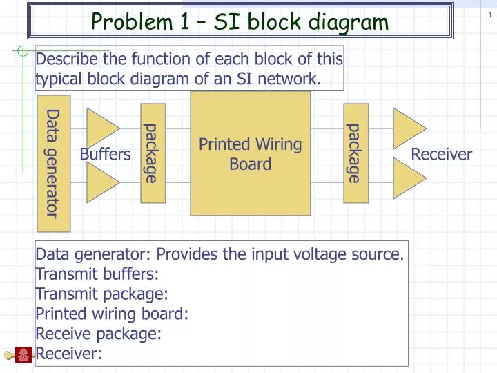
Printed Wiring Board. Data generator. package. package. Buffers. Receiver. Problem 1 – SI block diagram. Describe the function of each block of this typical block diagram of an SI network. Data generator: Provides the input voltage source. Transmit buffers: Transmit package:

E N D
Printed WiringBoard Data generator package package Buffers Receiver Problem 1 – SI block diagram Describe the function of each block of this typical block diagram of an SI network. Data generator: Provides the input voltage source. Transmit buffers: Transmit package: Printed wiring board: Receive package: Receiver:
Problem 2 – HSPICE pulse Given this pulse, write the HSPICE program Data rate 1V Pulse width 0 tr tf period 0 Answer: n+, n-, type, initial V, peak V, delay V1 ___ ___ ___ ___ ___ ____ + ___ ___ ___ ____ rise, fall, pulse width, period
Problem 3 – HSPICE circuit Given this HSPICE program, complete the circuit. Rin in Vss 1G Edrive out1 Vss VOL=V(in) Cout out1 Vss Tx_cterm Rout out1 out Tx_rterm Answer: in Rin 1G Vss
y Origin (of shape) Origin (of shape) -7.5 mil 2.5 mil 10.5 mil 10.5 mil x Origin (of coordinate system) Problem 4 – TL Field Solver Given this partial HSPICE program for a TL Field Solver, and this cross sectional view of the traces, fill in the CONDUCTOR settings: (SHAPE=_______, MATERIAL=_________, ORIGIN=___________) .MATERIAL brd_dielct2 DIELECTRIC ER=3.9 LOSSTANGENT=0.019 .MATERIAL brd_cu2 METAL CONDUCTIVITY=4.2E+07 .SHAPE brd_trap2 POLYGON + VERTEX = ( 0 0 ‘0.5*mil’ ‘0.5*mil’ ‘4.5*mil’ ‘0.5*mil’ ‘5*mil’ 0 ) .MODEL StripLines +W MODELTYPE=FieldSolver, LAYERSTACK=brd_sl_stk2 FSoptions=brd_opt2 +CONDUCTOR=(SHAPE= ? MATERIAL= ? ORIGIN=(‘ ? ’, ‘ ? ’)) +CONDUCTOR=(SHAPE= ? MATERIAL= ? ORIGIN=(‘ ? ’, ‘ ? ’)) +RLGCfile=StripLines.rlc .END Answer:
Problem 5 – Call subckt Assign the appropriate node names to the subcircuit figures, as shown by the call statements, in order to place the subcircuits into the main circuit. .SUBCKT PKG in1 in2 out1 out2 Vss L1 in1 out1 1n L2 in2 out2 1n .SUBCKT BRD in1 in2 out1 out2 Vss Wline1 in1 in2 Vss out1 out2 Vss XPKG_Tx pkg1_v pkg1_a + pkg1_vo pkg1_ao 0 PKG Xboard pkg1_vo pkg1_ao + pkg2_vo pkg2_ao 0 BRD ______ ______ ______ ______ Subckt BRD Subckt Pkg ______ ______ ______ ______
1V 0V 0 tr 1*dr 2*dr 3*dr 4*dr Problem 6 – PWL formulation Locate a, b, c, d, and e on the pwl figure below (tr=tf) *Bit pattern .param bit0=1 bit1=0 bit2=1 bit3=0 .SUBCKT Bitpattern data 0 VPWL data 0 PWL + 0 bit3 + ‘(tr*bit0)+(1-bit0)*tf’ bit0 + '1*datarate' bit0 + '1*datarate+(tr*bit1)+(1-bit1)*tf’ bit1 + '2*datarate' bit1 + '2*datarate+(tr*bit2)+(1-bit2)*tf' bit2 + '3*datarate' bit2 + '3*datarate+(tr*bit3)+(1-bit3)*tf' bit3 + '4*datarate' bit3 + r TD=0n a b c d e Answer: a