Download
1 / 20
570 likes | 3.92k Views
Design of 4-bit ALU. Ashwini Nanjappa Sravani Sanapala Vanita Ramaswamy Advisor: Dr.David Parent Fall 2004. Agenda. Abstract Introduction Why Simple Theory Project Details Block Diagram Schematics Layout Verification: DRC, Extract, LVS Simulation Results Cost Analysis Conclusion.

E N D
Design of 4-bit ALU Ashwini Nanjappa Sravani Sanapala Vanita Ramaswamy Advisor: Dr.David Parent Fall 2004
Agenda • Abstract • Introduction • Why • Simple Theory • Project Details • Block Diagram • Schematics • Layout • Verification: DRC, Extract, LVS • Simulation Results • Cost Analysis • Conclusion
Abstract • Aim of the project is to design a 4-bit ALU to perform seven arithmetic operations and four logic operations. • The circuit is designed so as to meet the following specifications: • Frequency: 200MHz • Power : 23W/cm2 • Area : 400x400µm2 • The results are verified with AMI06 technology, Spectre spice simulation tools.
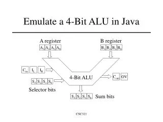
Introduction • ALU is a fundamental unit of several combinational circuits. Learning ALU design aids in designing complex circuits. • All the arithmetic operations are performed by the Carry look ahead adder using a B-input logic.The B-input logic is based on the equation Y=BiS0+Bi’S1 • The logic operations are performed using basic gates. • Two select lines are used to perform the operations on two 4 bit inputs in both the units. • The third select line is used to select either one of the units.
Introduction Cont’d. Function Table for ALU
Project Details • The B-input logic with CLA reduces the complexity of the circuit.The CLA consists of propagate/generate block, carry generator and sum block. • The critical path for the circuit is from the input B2 to the output out3 for the subtraction operation. • 4to1 Mux selects the logic operations based on the select lines in the logic unit. • Finally a 2to1 Mux selects between arithmetic and logic unit. • Mux based D-flipflops are used in the circuit with .7ns setup and hold time. • The sizing and layout of the gates are cell based.
Longest path has 17 logic levels including the input and output flipflops. A load of 20fF is assumed as the load for long path calculation from DFF. Long Path Calculation(Arithmetic Unit) τPHL=5ns/(13+4)=0.29ns for each logic level Project Details Cont’d
Logic Verified in NC-Verilog B-Input Logic Propagate/Generate CarryGenerator
ALU Test Bench Schematic The inputs (A,B,CIN) and select lines (M,S0,S1)are set for worst case.
Verification DRC Extracted LVSReport
CostAnalysis • Time is money ! • Time spent on each phase is: • Design and Implementation Phase: • Logic design and NC Verilog check– 1 Week. • Transitor level design and simulation – 2 Week. • Timing check, Stick Diagram and Layout- 1 week. • Verification and Testing Phase: • Post extraction, Power simulation & Time check - 1day
Designed and tested a 4 bit ALU that performs seven arithmetic and four logic operations at : 200 Mhz clock Power: 11.6W/cm2 Area: 333x412 μm2 The project meets all the given specifications This design concept can be a building block for higher bit ALU ex. 16-bit, 32-bit… Conclusion
Acknowledgement • Thanks to Professor David Parent for his guidance throughout the project. • Thanks to Cadence Design Systems for the VLSI lab. • Thanks to TA for helping us in the lab. • Thanks to our classmates.