Download
1 / 35
360 likes | 470 Views
Cache Memory and Performance. Many of the following slides are taken with permission from Complete Powerpoint Lecture Notes for Computer Systems: A Programmer's Perspective (CS:APP) Randal E. Bryant and David R. O'Hallaron http:// csapp.cs.cmu.edu/public/lectures.html

E N D
Cache Memory and Performance Many of the following slides are taken with permission from Complete Powerpoint Lecture Notes forComputer Systems: A Programmer's Perspective (CS:APP) Randal E. Bryant and David R. O'Hallaron http://csapp.cs.cmu.edu/public/lectures.html The book is used explicitly in CS 2505 and CS 3214 and as a reference in CS 2506.
An Example Memory Hierarchy L0: CPU registers hold words retrieved from L1 cache Registers L1: L1 cache (SRAM) L1 cache holds cache lines retrieved from L2 cache Smaller, faster, costlier per byte L2: L2 cache (SRAM) L2 cache holds cache lines retrieved from main memory L3: Main memory (DRAM) Larger, slower, cheaper per byte Main memory holds disk blocks retrieved from local disks Local secondary storage (local disks) L4: Local disks hold files retrieved from disks on remote network servers Remote secondary storage (tapes, distributed file systems, Web servers) L5:
Random-Access Memory (RAM) • Key features • RAM is traditionally packaged as a chip. • Basic storage unit is normally a cell (one bit per cell). • Multiple RAM chips form a memory. • Static RAM (SRAM) • Each cell stores a bit with a four or six-transistor circuit. • Retains value indefinitely, as long as it is kept powered. • Relatively insensitive to electrical noise (EMI), radiation, etc. • Faster and more expensive than DRAM. • Dynamic RAM (DRAM) • Each cell stores bit with a capacitor. One transistor is used for access • Value must be refreshed every 10-100 ms. • More sensitive to disturbances (EMI, radiation,…) than SRAM. • Slower and cheaper than SRAM.
SRAM vs DRAM Summary Trans. Access Needs Needs per bit time refresh? EDC? Cost Applications SRAM 4 or 6 1X No Maybe 100x Cache memories DRAM 1 10X Yes Yes 1X Main memories, frame buffers
Traditional CPU-Memory Bus Structure • A bus is a collection of parallel wires that carry address, data, and control signals. • Buses are typically shared by multiple devices. CPU chip Register file ALU System bus Memory bus Main memory Bus interface I/O bridge
Memory Read Transaction (1) • CPU places address A on the memory bus. Register file Load operation:movl A, %eax ALU %eax Main memory 0 I/O bridge A Bus interface A x
Memory Read Transaction (2) • Main memory reads A from the memory bus, retrieves word x, and places it on the bus. Register file Load operation:movl A, %eax ALU %eax Main memory 0 I/O bridge x Bus interface A x
Memory Read Transaction (3) • CPU read word x from the bus and copies it into register %eax. Register file Load operation:movl A, %eax ALU %eax x Main memory 0 I/O bridge Bus interface A x
Memory Write Transaction (1) • CPU places address A on bus. Main memory reads it and waits for the corresponding data word to arrive. Register file Store operation:movl %eax, A ALU %eax y Main memory 0 I/O bridge A Bus interface A
Memory Write Transaction (2) • CPU places data word y on the bus. Register file Store operation:movl %eax, A ALU %eax y Main memory 0 I/O bridge y Bus interface A
Memory Write Transaction (3) • Main memory reads data word y from the bus and stores it at address A. register file Store operation:movl %eax, A ALU %eax y main memory 0 I/O bridge bus interface A y
The Bigger Picture: I/O Bus CPU chip Register file ALU System bus Memory bus Main memory Bus interface I/O bridge I/O bus Expansion slots for other devices such as network adapters. USB controller Graphics adapter Disk controller Mouse Keyboard Monitor Disk
Storage Trends SRAM Metric1980 1985 1990 1995 2000 2005 2010 2010:1980 $/MB 19,200 2,900 320 256 100 75 60 320 access (ns) 300 150 35 15 3 2 1.5 200 DRAM Metric1980 1985 1990 1995 2000 2005 2010 2010:1980 $/MB 8,000 880 100 30 1 0.1 0.06 130,000 access (ns) 375 200 100 70 60 50 40 9 typical size (MB) 0.064 0.256 4 16 64 2,000 8,000 125,000 Disk Metric1980 1985 1990 1995 2000 2005 2010 2010:1980 $/MB 500 100 8 0.30 0.01 0.005 0.0003 1,600,000 access (ms) 87 75 28 10 8 4 3 29 typical size (MB) 1 10 160 1,000 20,000 160,000 1,500,000 1,500,000
The CPU-Memory Gap The gap widens between DRAM, disk, and CPU speeds. Disk SSD DRAM CPU
Locality • Principle of Locality:Programs tend to use data and instructions with addresses near or equal to those they have used recently • Temporal locality: • Recently referenced items are likely to be referenced again in the near future • Spatial locality: • Items with nearby addresses tend to be referenced close together in time
Locality Example • Data references • Reference array elements in succession (stride-1 reference pattern). • Reference variable sum each iteration. • Instruction references • Reference instructions in sequence. • Cycle through loop repeatedly. sum = 0; for (i = 0; i < n; i++) sum += a[i]; return sum; Spatial locality Temporal locality Spatial locality Temporal locality
Taking Advantage of Locality • Memory hierarchy • Store everything on disk • Copy recently accessed (and nearby) items from disk to smaller DRAM memory • Main memory • Copy more recently accessed (and nearby) items from DRAM to smaller SRAM memory • Cache memory attached to CPU
An Example Memory Hierarchy L0: CPU registers hold words retrieved from L1 cache Registers L1: L1 cache (SRAM) L1 cache holds cache lines retrieved from L2 cache Smaller, faster, costlier per byte L2: L2 cache (SRAM) L2 cache holds cache lines retrieved from main memory L3: Main memory (DRAM) Larger, slower, cheaper per byte Main memory holds disk blocks retrieved from local disks Local secondary storage (local disks) L4: Local disks hold files retrieved from disks on remote network servers Remote secondary storage (tapes, distributed file systems, Web servers) L5:
Caches • Cache:a smaller, faster storage device that acts as a staging area for a subset of the data in a larger, slower device. • Fundamental idea of a memory hierarchy: • For each k, the faster, smaller device at level k serves as a cache for the larger, slower device at level k+1. • Why do memory hierarchies work? • Because of locality, programs tend to access the data at level k more often than they access the data at level k+1. • Thus, the storage at level k+1 can be slower, and thus larger and cheaper per bit. • Big Idea: The memory hierarchy creates a large pool of storage that costs as much as the cheap storage near the bottom, but that serves data to programs at the rate of the fast storage near the top.
General Cache Concepts Smaller, faster, more expensive memory caches a subset of the blocks Cache 4 8 9 14 10 3 Data is copied in block-sized transfer units 4 10 Larger, slower, cheaper memory viewed as partitioned into “blocks” Memory 0 1 2 3 4 4 5 6 7 8 9 10 10 11 12 13 14 15
General Cache Concepts: Hit Data in block b is needed Request: 14 Block b is in cache: Hit! Cache 8 9 14 3 14 Memory 0 1 2 3 4 5 6 7 8 9 10 11 12 13 14 15
General Cache Concepts: Miss Data in block b is needed Request: 12 Block b is not in cache: Miss! Cache 8 9 14 3 12 Block b is fetched from memory Request: 12 12 • Block b is stored in cache • Placement policy:determines where b goes • Replacement policy:determines which blockgets evicted (victim) Memory 0 1 2 3 4 5 6 7 8 9 10 11 12 12 13 14 15
Types of Cache Misses • Cold (compulsory) miss • Cold misses occur because the cache is empty. • Conflict miss • Most caches limit blocks at level k+1 to a small subset (sometimes a singleton) of the block positions at level k. • E.g. Block i at level k+1 must be placed in block (i mod 4) at level k. • Conflict misses occur when the level k cache is large enough, but multiple data objects all map to the same level k block. • E.g. Referencing blocks 0, 8, 0, 8, 0, 8, ... would miss every time. • Capacity miss • Occurs when the set of active cache blocks (working set) is larger than the cache.
Examples of Caching in the Hierarchy Cache Type What is Cached? Where is it Cached? Latency (cycles) Managed By Registers 4-8 bytes words CPU core 0 Compiler TLB Address translations On-Chip TLB 0 Hardware L1 cache 64-bytes block On-Chip L1 1 Hardware L2 cache 64-bytes block On/Off-Chip L2 10 Hardware Virtual Memory 4-KB page Main memory 100 Hardware + OS Buffer cache Parts of files Main memory 100 OS Disk cache Disk sectors Disk controller 100,000 Disk firmware Network buffer cache Parts of files Local disk 10,000,000 AFS/NFS client Browser cache Web pages Local disk 10,000,000 Web browser Web cache Web pages Remote server disks 1,000,000,000 Web proxy server
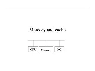
Cache Memories • Cache memories are small, fast SRAM-based memories managed automatically in hardware. • Hold frequently accessed blocks of main memory • CPU looks first for data in caches (e.g., L1, L2, and L3), then in main memory. • Typical system structure: CPU chip Register file ALU Cache memories System bus Memory bus Main memory Bus interface I/O bridge
Cache Performance Metrics • Miss Rate • Fraction of memory references not found in cache (misses / accesses)= 1 – hit rate • Typical numbers (in percentages): • 3-10% for L1 • can be quite small (e.g., < 1%) for L2, depending on size, etc. • Hit Time • Time to deliver a line in the cache to the processor • includes time to determine whether the line is in the cache • Typical numbers: • 1-2 clock cycle for L1 • 5-20 clock cycles for L2 • Miss Penalty • Additional time required because of a miss • typically 50-200 cycles for main memory (Trend: increasing!)
Lets think about those numbers • Huge difference between a hit and a miss • Could be 100x, if just L1 and main memory • Would you believe 99% hits is twice as good as 97%? • Consider: cache hit time of 1 cyclemiss penalty of 100 cycles • Average access time: 97% hits: 1 cycle + 0.03 * 100 cycles =4 cycles 99% hits: 1 cycle + 0.01 * 100 cycles = 2 cycles • This is why “miss rate” is used instead of “hit rate”
Measuring Cache Performance • Components of CPU time • Program execution cycles • Includes cache hit time • Memory stall cycles • Mainly from cache misses • With simplifying assumptions:
Cache Performance Example • Given • I-cache miss rate = 2% • D-cache miss rate = 4% • Miss penalty = 100 cycles • Base CPI (ideal cache) = 2 • Load & stores are 36% of instructions • Miss cycles per instruction • I-cache: 0.02 × 100 = 2 • D-cache: 0.36 × 0.04 × 100 = 1.44 • Actual CPI = 2 + 2 + 1.44 = 5.44 • Ideal CPU is 5.44/2 =2.72 times faster
Average Access Time • Hit time is also important for performance • Average memory access time (AMAT) • AMAT = Hit time + Miss rate × Miss penalty • Example • CPU with 1ns clock, hit time = 1 cycle, miss penalty = 20 cycles, I-cache miss rate = 5% • AMAT = 1 + 0.05 × 20 = 2ns • 2 cycles per instruction
Performance Summary • When CPU performance increased • Miss penalty becomes more significant • Decreasing base CPI • Greater proportion of time spent on memory stalls • Increasing clock rate • Memory stalls account for more CPU cycles • Can’t neglect cache behavior when evaluating system performance
Multilevel Caches • Primary cache attached to CPU • Small, but fast • Level-2 cache services misses from primary cache • Larger, slower, but still faster than main memory • Main memory services L-2 cache misses • Some high-end systems include L-3 cache
Multilevel Cache Example • Given • CPU base CPI = 1, clock rate = 4GHz • Miss rate/instruction = 2% • Main memory access time = 100ns • With just primary cache • Miss penalty = 100ns/0.25ns = 400 cycles • Effective CPI = 1 + 0.02 × 400 = 9
Example (cont.) • Now add L-2 cache • Access time = 5ns • Global miss rate to main memory = 0.5% • Primary miss with L-2 hit • Penalty = 5ns/0.25ns = 20 cycles • Primary miss with L-2 miss • Extra penalty = 400 cycles • CPI = 1 + 0.02 × 20 + 0.005 × 400 = 3.4 • Performance ratio = 9/3.4 = 2.6
Multilevel Cache Considerations • Primary cache • Focus on minimal hit time • L-2 cache • Focus on low miss rate to avoid main memory access • Hit time has less overall impact • Results • L-1 cache usually smaller than a single cache • L-1 block size smaller than L-2 block size