Download
1 / 26
260 likes | 266 Views
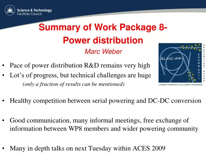
Summary of Work Package 8- Power distribution Marc Weber. Pace of power distribution R&D remains very high Lot’s of progress, but technical challenges are huge (only a fraction of results can be mentioned) Healthy competition between serial powering and DC-DC conversion

E N D
Summary of Work Package 8- Power distribution Marc Weber • Pace of power distribution R&D remains very high • Lot’s of progress, but technical challenges are huge • (only a fraction of results can be mentioned) • Healthy competition between serial powering and DC-DC conversion • Good communication, many informal meetings, free exchange of information between WP8 members and wider powering community • Many in depth talks on next Tuesday within ACES 2009
reduce current through power cables by a) “recycling” of current (SP) oder b) “high-voltage power transmission (DC-DC) How to get the power in ? Serial powering DC-DC buck converter DC-DC charge pump Piezo transformer Power supply
Some highlights of DC-DC conversion R&D • Progress on radiation-hard technologies • Lot’s of progress on DC-DC topology choices and converter design • Convergence on Two-stage conversion scheme • Custom air-coil inductors with PCB technology • Integrated DC-DC charge pumps • Wealth of test results with large-scale silicon detectors
Semiconductor technology (1) • The converter requires the use of a technology offering both low-voltage and high-voltage (15-20V) transistors • Properties of high-voltage transistors largely determine converter’s performance • Need for small Ron, and small gate capacitance (especially Cgd) for given Ron! • Survey of available options covered 5 technologies • Best results with 0.25um SGB25V GOD technology from IHP Prototype in 0.35mm F.Faccio, PH/ESE
ASIC development – 2nd generation • Second generation prototype • Still manufactured in AMIS 0.35mm • Features: • VIN and Power Rail Operation from +3.3V to +12V • Selectable output voltage (nominal 2.5V) • Maximum output current: 3A • Fast Transient Response - 0 to 100% Duty Cycle • 14MHz Bandwidth Error Amplifier with 10V/μs Slew Rate • Internal oscillator fixed at 1Mhz, programmable from 400kHz to 3MHz with external resistor • Internal voltage reference (nominally (1.2V) • Remote Voltage Sensing with Unity Gain • Programmable delay between gate signals • Integrated feedback loop with bandwidth of 20Khz • Submitted December 08, expected back in April 09 • Mounted in 7x7mm QFN package • Third generation will be in the IHP 0.25mm technology • It will be a simple buck • Refined comparison with 2-phase interleaved with V-divider (alternative topology), using also prototypes, has indicated little advantage of this latter topology at the small load currents foreseen for a module F.Faccio, PH/ESE
Proposed distribution scheme (ATLAS Short Strip concept) Rod/stave 10-12V Voltage for SC and optoelectronics generated locally by a converter stage 1 2 Converter stage2 on-chip • Scheme based on 2 conversion stations: • Stage 1 at the module level • Stage 2 on-chip Summary of features • Modular approach, very flexible – building blocks can be custom assembled following system requirements • Each module turned on-off independently by SC • Each FE chip turned on-off independently by HC • Easy, gradual detector turn on procedure • Conventional grounding scheme • Conventional detector powering • Very efficient to provide only required power to every system component, at appropriate voltage Detector Hybrid controller Intermediate voltage bus(ses) 10-12V Converter stage 1 block F.Faccio, PH/ESE
“Optimized” PCB toroid (1) • Custom design exploiting PCB technology: easy to manufacture, characteristics well reproducible • Design can be optimized for low volume, low ESR, minimum radiated noise • With the help of simulation tools (Ansoft Maxwell 3D and Q3D Extractor), we estimated inductance, capacitance and ESR for different designs. This guided the choice of the samples to manufacture as prototypes • The addition of two Al layers (top, bottom) shields the parasitic radiated field efficiently F.Faccio, PH/ESE
Toroid not shielded solenoid Noise floor Shielded toroid “Optimized” PCB toroid (2) • First samples manufactured at the CERN PCB shop • Inductance, shield efficiency, ESR in agreement with simulation • ESR can be decreased still by 2x by “filling” the vias – this has not yet been done • Now that the concept has been validated, we prepare for a prototype run with all the final characteristics (ESR, volume, shield material) Measurement in the lab: Normalized current induced in 1 Cu loop at increasing distance from the inductor (cm) F.Faccio, PH/ESE
System Test with a TEC Petal < Lutz Feld (RWTH Aachen)
System Test with Commercial DC-DC Converters • internal or external ferrite core inductor: 10% noise increase • air-core inductor: huge noise increase, interference with module both radiative and conductive • “radiative part” can be reproduced by an air core coil converter (not connected to a module) above hybrid • “conductive part” can be reproduced by noise injection into the cables (see later) • No converter • Internal inductor • External ferrite inductor • External air-core inductor • Ext. air-core inductor + LDO Pos. 6.2 radiative part conductive part Lutz Feld (RWTH Aachen)
Some highlights of serial powering R&D • Serial powering supermodule system architecture much better understood • Protection schemes are emerging • Custom shunt regulator circuitry became available and seems to be functional • AC – LVDS coupling of data and control and command signals much better understood
SP with commercial electronics 1) Supermodule with SP (LBNL and RAL) PCB with SP circuitry, 38 mm x 9 mm BeO MCM and SP PCB Results: 1) no noise, robust system 2) Can bias sensors with a common HV line 3) AC (Multidrop) LVDS working well 2) Large supermodule with SP 30 MCMs with SP 11 Sensoren Results : 4) Long SP chain working well
Supermodule architecture ~1.2m
Need radiation-hard SP ASICs with small dynamic impedance. Which architecture is best? Each ABC-N has its own shunt regulator & transistor(s) SP ASIC Design: ABC-Next and SPi Just one shunt regulator – Use each ABC-N transistor(s) W scheme M scheme SPi scheme Just one shunt regulator and transistor SR = Shunt regulator Linear regulators and other connections omitted New territory for particle physics. Great interest of IC designers
ABC-Next with SP blocks for W and M scheme Both schemes are being evaluated. Preliminary tests on single chips (rather than hybrid) are looking good. Chips and SP blocks are functional and noise performance is OK
SP made easy - the SPi IC SPi is stand-alone IC with all relevant SP elements: 1) Shunt regulator 2) Shunt transistor 3) LVDS ports plus - Shunt current sensing ADC - Over-current protection - Linear regulators suitable for 1.2 V to 2.5 V technology: TSMC 0.25m CMOS area: ~ 14 mm2 max. current through shunt transistor: 1-3 A SPi makes SP straightforward.
Richard Holt – Rutherford Appleton Laboratory ATLAS SCT SP protection options January 2009 Why add protection? Power failure modes Open circuit module Wire bonding failure Noisy module Without protection, one failed module can adversely affect the operation of all other modules on stave Demonstration staves are very reliable - Protection is not strictly necessary 2
SCR Serial powering sceme MPC = on I in = 3,6 A DCS on EOSC I = 0,8 * 4 chips = 3,6 A local VDD D1 MPC1 4chipsmodule D2 + simple + control & monitor + fast auto-response default state = OC - 1 AWG 36 line / module I out = 3.6 A R D3 4chipsmodule MPC2 local GND 4chipsmodule MPCx OC = Open Circuit (ie switch is “off”, module powered) 15
Need both analog and digital voltage How? There are many choices. So far Vanalog < Vdigital in future : Vanalog = 1.2 V, Vdigital = 0.9 V Efficiency =: ABC-N power consumption/total consumption at rack power supply No DC-DC Highestefficiency H 70% 81% No DC-DC 72% 56% Highestvoltage 72% 79% • SR = Shunt Regulator, LR = Linear Regulator, • DC-DC = DC to DC voltage conversion
Possible schema of power management in ABCN (130 nm) 3 vddd 0.9 V Vdd(a) 1.5V Fully integrated ShuntRegulator Voltage Regulator ABCN Analoge DC-DC Charge pump ABCN Digital 1.2V gnda gndd Design study carried out by M. Bochenek Possibly most efficient system compatible with serial powering
Power efficiency IP 24 cables for digital power, 24 cables for analog. Also “sense wires”. (Ianalog = 0.32 A, Idigital = 1.02 A, cable resistance (both ways) 2 Ohms) Efficiency =: ABC-N power consumption/total consumption (cables, regulator, ABC-N) Independent powering (100% hybrid efficiency) 1 stave = 24 hybrids = 480 ABC-N (0.13 m) Power (voltage) 2.63 kW 3 Watts 2.66 kW 0 Watts 32 Watts Efficiency = 1% D
Power efficiency SP 1 cable for digital plus analog current. Only minimal cable losses! Serial powering a stave, (higher voltage, with DC-DC / 2 for digital) 1 stave = 24 hybrids = 480 ABC-N (0.13 m) Power (constant current) 2.2 Watts 0.5 Watts 42 Watts 8.8 Watts (79% efficiency ) H 32 Watts Efficiency = 73% D Cables assumed to be 2 ohms total for each power line pair Regulator power = (1/eff - 1) x ABC power H Stave supply current = (32 + 8.5)watts / (1.6volts x 24) = 1.1amps Numbers rounded
Summary and next steps • Characterize various ASICs designs for both DC-DC and SP • Move on to more realistic technologies (e.g. 130 nm CMOS) • Understand system architecture better • Gain practical experience with “full system” prototypes (sensors, readout chips, hybrids, modules, supermodules) Huge progress, but The more progress we make, the larger the challenge seems to become…Still looking good