Download
1 / 31
310 likes | 319 Views
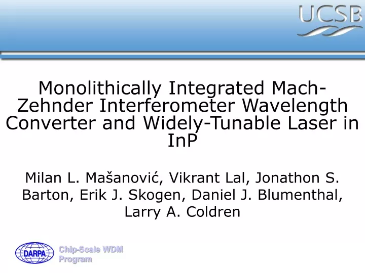
Milan L. Mašanović, Vikrant Lal, Jonathon S. Barton, Erik J. Skogen, Daniel J. Blumenthal, Larry A. Coldren. Monolithically Integrated Mach-Zehnder Interferometer Wavelength Converter and Widely-Tunable Laser in InP. Summary of Work. Objective/scope

E N D
Milan L. Mašanović, Vikrant Lal, Jonathon S. Barton,Erik J. Skogen, Daniel J. Blumenthal, Larry A. Coldren Monolithically Integrated Mach-Zehnder Interferometer Wavelength Converter and Widely-Tunable Laser in InP
Summary of Work • Objective/scope • Demonstrate InP monolithic integration of a widely tunable laser and all-optical wavelength converter for digital and analog wavelength conversion. • Approach • Utilize a common offset quantum well integration platform and a combination of passive, active and filter waveguides to implement on a single chip a Mach-Zehnder SOA Interferometer and widely tunable SGDBR laser. • Major accomplishments • Demonstration and testing of world’s first monolithically integrated tunable laser and AO wavelength converter • Wide conversion range: 50+nm in, 22nm (L-Band) • 2.5GB/s error free operation • Issues • SGDBR on-chip output power and mirrors • Passive waveguide losses, chip insertion losses • SOA speed (gain recovery) • C-Band operation
Monolithically Integrated InP AOTWC Sampled Grating DBR Laser Mach-Zehnder Interferometer Input Amplifier
Integration Challenges • Enable a Common Fabrication Platform • Offset Quantum Wells • Tradeoffs Between Laser and MZI Performance • Optical Isolation • Lasers Highly Sensitive to Coherent Reflections • Active/Passive Interfaces • Amplified Reflections • Facet Reflections Need to be Suppressed Effectively (10-5 or better) • Processing Issues • Material Quality - Uniformity • Processing Uniformity - Very Long Devices
Front Mirror Gain Phase Rear Mirror Offset QW Device SGDBR Laser Background • 4 Section Device • Wide Tunability, High Power • Suitable for Integration • Passive – Active Waveguide Combination • Does not Require Facet Reflection to Lase • Realized in Several Integration Platforms(*) • Offset Quantum Wells • Burried Ridge Stripe (OQW, QWI) *Beck Mason, Erik Skogen, Larry Coldren
Transfer Function SOA Current Optical Power Cross-Phase Modulation Principle π phase shift No CW light out CW in • Semiconductor optical amplifiers used to achieve phase shift • Incoming data disturbs phase balance data conversion π phase shift Data in Converted Signal Out CW in Inverting Operation Non Inverting Operation Interferometer - Cross Phase Modulation
1- 1x2 MMI Splitter/Combiner 1- 1x2 MMI Splitter/Combiner 2- 2x2 MMI Coupler 2- S Bend 3 - MQW SOA 3 - MQW SOA 3 2 2 1 1 2 3 1 1 1 2 2 3 Generation I Interferometer Designs • Two different interferometer realizations • MMI/S Bend Design • 2 Stage MMI Design
1515 nm 1545 nm 1575 nm MMI Components • Function • N*N power splitting/coupling • Most common components: • 1x2, 2x1 splitter/combiner • 2x2 (3dB) coupler • Properties • Simple Structure and Fabrication • Low Inherent Loss • Large Bandwidth • Low Polarization Dependence
Width Taper 7° Angle 5 µm Facet Reflections • Depending on the SOA Gain, Maximum Tolerable Reflection R=0.251.25 10-4 • Optimized Output Waveguide Required • Multilayer (3) AR Coating
Thermal Consideration – Interferometer Design • Thermal Crosstalk • Affects power/gain/dynamics • 80 μm SOA Spacing • Tradeoff between device length and temperature effects
Active – Passive Removal Grating Formation InP/InGaAs Regrowth Metalization/Anneal Passivation/Implant Ridge Etch Offset Quantum Well Process Most Mature SGDBR Fabrication Technology Requires Single MOCVD Regrowth
Actual Device Layout (Active and Ridge Layer Shown) Active Regions Critical Steps - Verification • Active Regions Removal PL Line Scan • Gratings Etch AFM Scan
5 um First Generation Tunable Wavelength Converter
Gain Bandwidth and Tuning Range Gain Peak – 1560nm Tuning Range – 22nm
Mirror Design • Mirror • Carrier Injection Cause for Index Change (7nm) • Gen 1 Mirror • Patchy Band Coverage • Irregular Supermode Tuning • Grating pitch – L-band lasers • Gen 2 Mirror • Problem Fixed
Electrical/Optical Control Optical Control Electrical Control
DC Extinction Map • Higher Extinction For low bias currents
Difference in SOA Output Power Strongly Affects Extinction Keep Powers Equal in Both Branches and Change Phase Independently Power-Extinction Analysis
SOA Phase Change of Pi Required High Speed Operation – Lower Index Change Extend the SOA Length Phase-Extinction Relation
Back-to-back Data Gen. PC PC Device BPF EDFA BPF λin EOM λout BER EDFA BPF Attenuator PD Error Rate Pin Test Setup
2.5GB/s Conversion – Fixed SGDBR Wavelength 1535nm 1565nm Input Eye Diagram PRBS 231-1 1545nm 1575nm Converted Data 1585nm 1555nm
2.5GB/s Conversion – Fixed Input Wavelength Input Eye Diagram PRBS 231-1 1557nm 1566nm Converted Data 1578nm 1570nm
2.5GB/s Bit Error Rate Testing Fixed SGDBR Output Wavelength PRBS 231-1 Input ~2dB Power Penalty 2dB
First Generation WC Performance Limits 5GB/s Eye λin=1590nm 2.5GB/s +4mW SGDBR Power Difference 1mW
Mirror Design Tuning Range Low MZI Input Power (<0.8mW) Improve Electrical and Optical Extinction Improve conversion efficiency (input to output) Speed up Carrier Dynamics Summary of Issues to be Resolved
Second Generation WC Design • Improvements • Redesigned Mirrors • Wider tuning range • Better ‘behavior’ • Output Coupler • Light Evacuation • Phase Control • Improved Extinction • Input SOAs • Boost Input Power • Reduce Lifetime • 1.4Q Waveguide • Higher Output Power
Second Generation WC with TIR Mirror • TIR Mirror • Insertion Loss • ~200μm propagation • Distortion • No SOA at the input • SNR • Eliminated extra ASE
Requirements for High Speed Wavelength Conversion • Requirements • Small Optical Area • Large Confinement • High Differential Gain • Long Length • High Bias Current • Buried Ridge Stripe using QWI • Improved Confinement • Reduced Losses/Reflections • Reduced Heating
Summary • Major accomplishments • Demonstration and testing of world’s first monolithically integrated tunable laser and AO wavelength converter • Wide conversion range: 50+nm in, 22nm (L-Band) • 2.5GB/s error free operation • Future Work • Fabricate Second Generation Devices • Analog Characterization for Gen I Devices • Compare Performance (Digital/Analog)