Download
1 / 18
180 likes | 183 Views
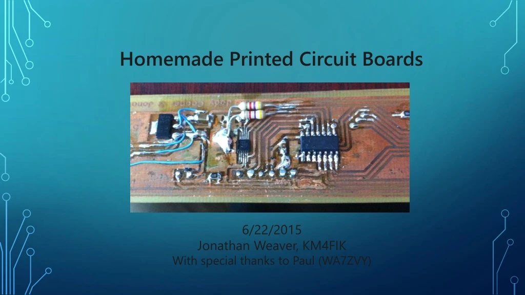
Learn how to create PCB artwork, transfer it to copper, and etch your own circuit boards at home. Includes step-by-step instructions and recommended suppliers.

E N D
Homemade Printed Circuit Boards 6/22/2015 Jonathan Weaver, KM4FIK With special thanks to Paul (WA7ZVY)
Overview • Creating PCB Artwork • Getting the PCB Artwork to copper • Preparation before Etching • Etching • Work after Etching • Supplies and Suppliers
Creating PCB Artwork: Circuit Design • Find and use • Magazines, books, and references • Online • Component datasheets • Find and modify • Use specialized tools (logic tools, filter tools, etc) • Create from Scratch More Knowledge and Experience
Creating PCB Artwork: Circuit Simulation • Verify that it “works” • Tool: LTSpice (freeware downloadable at www.linear.com/ltspice) • Alternative: Pspice Student, OrCAD Lite (free versions of production software with limitations)
Creating PCB Artwork: Schematic • Easy to read • Incorporates notes • Generates a bill of materials (list of parts) • Generates a net list (how the parts are connected) • Tools: TinyCAD (http://sourceforge.net/projects/tinycad/) • Alternative Tools: • ExpressPCB (easiest to learn) • Eagle (freeware has limitations, but very popular) • KiCAD • GEDA (Linux only) • DesignSpark PCB
Creating PCB Artwork: PCB Layout • Physical Layout • 600 dpi printing limits the minimum sizes • 15 to 20 mil (1/1000 inch) trace width where possible. 5 mil trace width minimum (3 dots) • Similar on spacing • 30 to 40 mil holes on 55 to 60 mil pads • Use copper “fill” areas to minimize etching • Imports net list (parts and hookups) • Includes an auto router (I usually never use) • Generates manufacturing files (usually Gerbers)
Creating PCB Artwork: PCB Layout Cont.d • Free PCB plus ViewMate Gerber Viewer • Alternatives: • ExpressPCB (easiest to learn but tied to vendor if you want PCB's manufactured) • Eagle (freeware has limitations) • KiCAD • GEDA (Linux only) • DesignSpark PCB • At this point you can send the PCB files to a manufacturer or etch a board yourself
Printing a PCB • Print to verify size, etc. • Print for etching (to PDF using PDF Creator) • Mirror the top side • Bottom side is already mirrored • Keep the PDF file for easy printing later on • Print using LASER printer on magazine paper • Alternative papers include • Epson Glossy Ink Jet Photo Paper P/N S041141 • Pulsar Toner Transfer System (http://pulsarprofx.com). Digikey P/N 182-1003-ND and P/N 182-1021-ND. • Line up top and bottom using light under glass table or light table • Tape two sides down
Getting the PCB Artwork to Copper • Clean the copper clad board with a scotchbrite pad • Insert the board in the print out “pocket” • Iron on high. Cover entire board with iron. About a minute. Apply good pressure (I usually iron on a counter top). • Let board “sandwich” cool (sets the ink to the copper). • Soak the “sandwich” in a sink of cool water • Gently remove paper. Use toothbrush or sponge to remove small bits of paper stuck to the ink.
Board Prep before Etching • Inspect!!!! • Use an Exacto knife to cut any "shorted" traces or pins apart. • Use a fine point sharpie marker to draw in traces that may have been lifted with the paper removal. • If it is unrepairable, clean off failed transfer with Acetone, and start over. • Cut out the board with a Dremel tool (SAFETY GLASSES). Use care not to scratch the design.
Etching • Bath of hot water • Float bath of etchant (Ferrious Chloride) • SAFETY TOOLS: Latex gloves, safety glasses, apron or disposable clothes (etchant stains) • Submerge PCBs. Agitate Etchant. Flip PCBs. • Repeat until all exposed copper is removed. • Submerge PCBs in cold water to remove etchant and stop chemical reaction • Dry PCBs.
After Etching • CLEAN UP – I store used etchant and reuse. Etchant can be neutralized with wash powder, dilluted, and disposed down the drain. • Clean ink off the PCB using acetone (nail polish remover) and scotchbrite pad. • Drill holes with drill press (etched holes in pads help line up the bit) • Solder vias through holes (use bare bus wire) • Solder components and jumpers (soldering would be a whole other presentation)
Suppliers • Parts • Digikey (www.digikey.com) • Jameco (www.jameco.com) • Mouser (www.mouser.com) • Others (Radioshack, Element 44, Allied, etc) • Copper Clad boards and drill bits • Far Circuits (www.farcircuits.net) operated by KF9GX • He will also etch your boards for you • He accepts ExpressPCB files