Download
1 / 11
120 likes | 323 Views
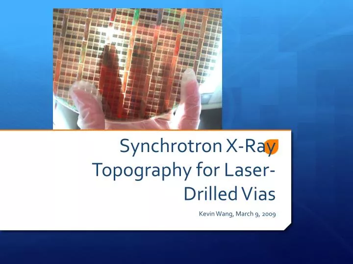
Synchrotron X-Ray Topography for Laser-Drilled Vias. Kevin Wang, March 9, 2009. Through Silicon Via. Via connecting one side of silicon wafer to another Reduce connection length Drilling options Mechanical Deep Reactive Ion Etching (DRIE) Laser pulses.

E N D
Synchrotron X-Ray Topography for Laser-Drilled Vias Kevin Wang, March 9, 2009
Through Silicon Via • Via connecting one side of silicon wafer to another • Reduce connection length • Drilling options • Mechanical • Deep Reactive Ion Etching (DRIE) • Laser pulses DRIE Vias, Source: Albany Nanotech
Paper • Laser Drilled Through Silicon Vias: Crystal Defect Analysis by Synchrotron X-ray Topography • Landgraf, R., Rieske, R., Danielewsky, A., Wolter, K. • TechnischeUniverstät Dresden, Germany • Synchrotron Source: ANKA (Karlsruhe, Germany) • 2.5 GeV,current 80-180 mA: white radiation 2Å • Presented at: • 2nd Electronics System-Integration Technology Conference, Greenwich, UK (2009-09-01)
DRIE vs. Laser Drilling DRIE Vias, Source: Lam Research Laser Via, Source: Landgraf Sidewall Scalloping, Source: Aviza Technology
Laser Via Fabrication • 525μm thick Si wafer (100) • 4in. (100mm) • Target via diam: 50 μm
Laser Drilling Methods • Single Pulse • Trepanning (cut an annulus) • Percussion (high power pulsing) Conventional drilling patterns, Source: Verhoeven, K.
X-ray Diffraction Setup • Section Transmission (15μm slit), Lang Method
Results – Strain Imaging ps laser: 290μmstrain zone ns laser: 540 μmstrain zone
Trend with Laser Pulse Width • Strain affected region: • Distance from via edge to strain edge fs laser: 220μmstrain zone
Conclusion • Transmission topography by synchrotron source successfully imaged strain near vias, nondestructively • Strain affected zone decreased with pulse width • Electron-phonon relaxation time in Si, 400fs • Femtosecond lasers should be considered for commercial production • Depth remains to be improved
Motivation: Multi-Chip Packages • Wirebonding • Longer paths • Failure due to fatigue, bond lifting • Flipchip bumps • Reduce path length • Still require redistribution layer (RDL) • Thermal cycling failure Wirebonded Die, Source: Aspen Tech. Flipchip Die, Source: IMEC