Download
1 / 18
180 likes | 301 Views
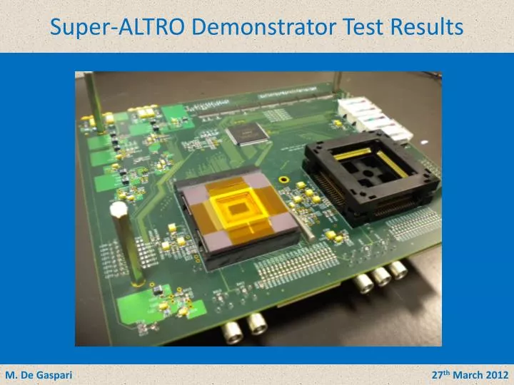
Super-ALTRO Demonstrator Test Results. M. De G aspari. 22 nd November 2011. 27 th March 2012. LC Power Distribution & Pulsing Workshop, May 2011. Introduction. First test results already presented in October 2011, see:

E N D
Super-ALTRO Demonstrator Test Results M. De Gaspari 22nd November 2011 27th March 2012 LC Power Distribution & Pulsing Workshop, May 2011 LC Power Distribution & Pulsing Workshop, May 2011
Introduction • First test results already presented in October 2011, see: • http://ilcagenda.linearcollider.org/materialDisplay.py?contribId=3&materialId=slides&confId=5365 • Or see: • http://indico.cern.ch/conferenceDisplay.py?confId=155595 • New test conditions: • Sampling clock frequency increased to 40MHz (design target), readout clock 40MHz. • Chip PGA3: the inputs of the PASA are not bonded. This avoids noise injection from the ground plane of the test board. • Chip PGA4: all inputs bonded. • Measurements presented today: • Analog noise • Digital power consumption • Chip power consumption and power pulsing measurements M. De Gaspari 22nd November 2011 27th March 2012 LC Power Distribution & Pulsing Workshop, May 2011
Acquired pulses Examples of acquisitions at 30ns and 120ns shaping time. Sampling frequency 40MHz. Signal scan with a granularity of 5ns. M. De Gaspari 22nd November 2011 27th March 2012 LC Power Distribution & Pulsing Workshop, May 2011
Gain measurement PASA configuration: 12mV/fC, 120ns, High polarity Measured gain 10.6mV/fC±1.9% M. De Gaspari 22nd November 2011 27th March 2012 LC Power Distribution & Pulsing Workshop, May 2011
Baseline noise: PGA3 PGA3: inputs not bonded Noise constant across channels M. De Gaspari 22nd November 2011 27th March 2012 LC Power Distribution & Pulsing Workshop, May 2011
Noise summary Measured baseline noise averaged over 16 channels. Shaping 30-120ns, Gain 12-27mV/fC, signal polarity H/L. (H = negative input charge => MPGD, L = positive input charge => wire chamber) M. De Gaspari 22nd November 2011 27th March 2012 LC Power Distribution & Pulsing Workshop, May 2011
Baseline noise: PGA4 Measured baseline noise for different input capacitances. PGA4, Channel 0, 120ns, 12mV/fC M. De Gaspari 22nd November 2011 27th March 2012 LC Power Distribution & Pulsing Workshop, May 2011
Baseline noise: DSP influence (PGA4) Negligible influence of the amount of switching logic on the noise: basic data acquisition and data acquisition with BC1 memory (Look-Up Table) switching. M. De Gaspari 22nd November 2011 27th March 2012 LC Power Distribution & Pulsing Workshop, May 2011
DSP tests 1 Known pattern written in the Pedestal Memory (Baseline Correction 1) and used as test input Drift of the baseline Undershoots Emulates the pattern produced by a real detector M. De Gaspari 22nd November 2011 27th March 2012 LC Power Distribution & Pulsing Workshop, May 2011
DSP tests 2 The DSP removes offsets, undershoots, baseline drifts M. De Gaspari 22nd November 2011 27th March 2012 LC Power Distribution & Pulsing Workshop, May 2011
Power consumption: DSP Power consumption of the DSP when acquiring at 40MHz sampling frequency. Different DSP functionalities included. M. De Gaspari 22nd November 2011 27th March 2012 LC Power Distribution & Pulsing Workshop, May 2011
Power consumption: DSP Power consumption of the DSP for different sampling clock frequencies. DSP configuration: (Data In) – (Look-Up Table). M. De Gaspari 22nd November 2011 27th March 2012 LC Power Distribution & Pulsing Workshop, May 2011
Power consumption: DSP Power consumption of the DSP at different supply voltages. Efficient operation down to 1V supply. M. De Gaspari 22nd November 2011 27th March 2012 LC Power Distribution & Pulsing Workshop, May 2011
Power consumption Each block can be switched off independently, and without removing the supply voltage (smart shutdown). PASA and ADC: remove the bias voltages DSP: remove the sampling/readout clock Power per block (mW) Power consumption: 47.3mW/ch, 757mW total @40MHz. M. De Gaspari 22nd November 2011 27th March 2012 LC Power Distribution & Pulsing Workshop, May 2011
Power pulsing cycle Acquisition Readout Power up L1 Trigger Power consumption of the DSP during a power pulsing cycle. Minimum delay between power up and L1 trigger has to be measured. Readout time is determined by the test setup (RCU) minimum PP cycle ≈1ms. M. De Gaspari 22nd November 2011 27th March 2012 LC Power Distribution & Pulsing Workshop, May 2011
Power pulsing cycle Good region Continuous mode A test pulse is injected after power up; the amplitude of the pulse is monitored with different delays between power up and L1. 100usec delay gives good results: difference with continuous mode <1LSB M. De Gaspari 22nd November 2011 27th March 2012 LC Power Distribution & Pulsing Workshop, May 2011
Power pulsing: results Power pulsing cycles are repeated at a frequency of 50Hz (Duty≈1/20). Chip total power=9.2mW+50Hz*654.3uJ=41.9mW Power reduction by a factor 18.1! (continuous mode: 757mW) M. De Gaspari 22nd November 2011 27th March 2012 LC Power Distribution & Pulsing Workshop, May 2011
Conclusions • The 16 channel Super-ALTRO Demonstrator has been designed, prototyped and tested successfully!! • The chip is already usable for the Linear Collider TPC prototype. • The area is 3.07mm2/channel (LCTCP requirement: <4mm2) • Using appropriate design techniques, integration of low-noise analog components and digital functions is possible with little effect on noise performance. • Power pulsing approach has been demonstrated effective in reducing the power consumption, while preserving the performance. M. De Gaspari 22nd November 2011 27th March 2012 LC Power Distribution & Pulsing Workshop, May 2011