Download
1 / 4
40 likes | 43 Views
There are more and more included in the market and more and more incorporated in electronics but what are the advantages of HDI PCBs

E N D
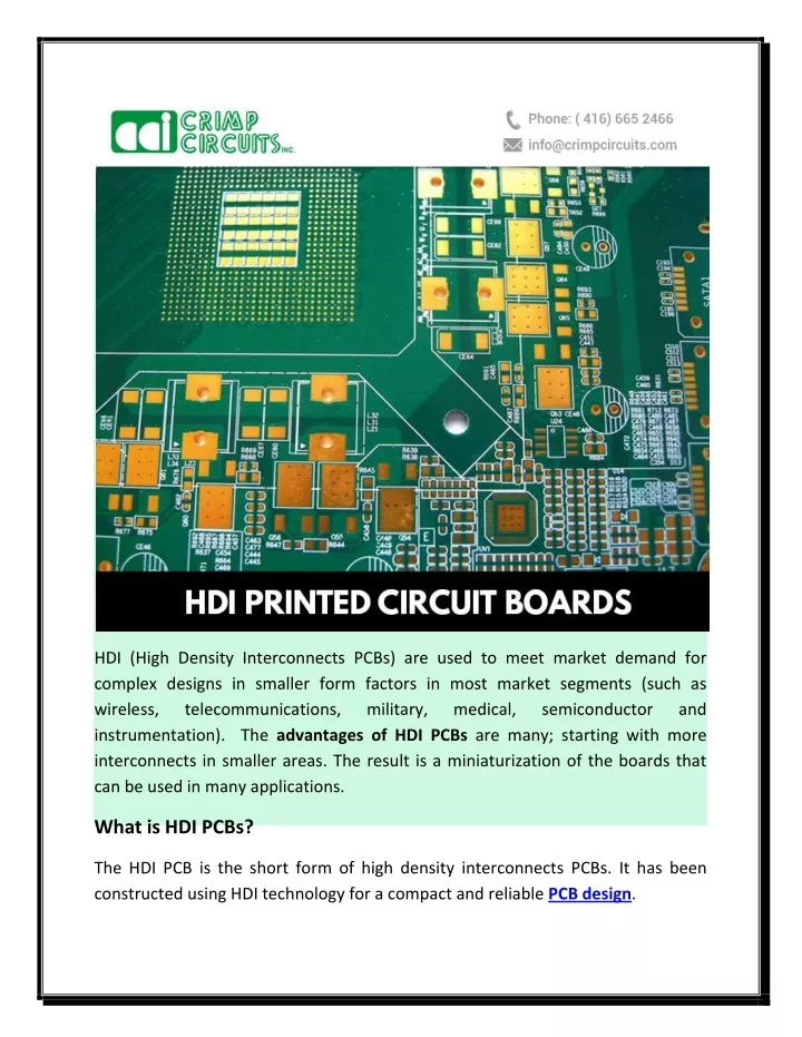
HDI (High Density Interconnects PCBs) are used to meet market demand for complex designs in smaller form factors in most market segments (such as wireless, telecommunications, military, instrumentation). The advantages of HDI PCBs are many; starting with more interconnects in smaller areas. The result is a miniaturization of the boards that can be used in many applications. medical, semiconductor and What is HDI PCBs? The HDI PCB is the short form of high density interconnects PCBs. It has been constructed using HDI technology for a compact and reliable PCB design.
It features high-density attributes, including laser micro-via, fine lines and high- performance materials. Conventional PCBs are coated with copper in the inner and outer layers, or like HDI PCBs are incorporated with stacked micro-via-filled multi-copper layers. Components are placed closer together and space on the board is significantly reduced, but functionality is not compromised. This creates a structure allowing complex interconnections to provide the necessary routing solutions. High-tech applications use the advantages of HDI PCBs to build high pin count chips. Benefits of HDI PCBs Due to the evolution of HDI PCB technology, there is more freedom and flexibility to design applications according to consumer demands. They have more space to place components on both sides of the raw PCB The main advantages of this technology are: Heat transfer is reduced due to the proximity of the components. Thermal expansion of the HDI PCB is also less stressed and increases endurance. Better conductivity management: The ventilation holes of the HDI PCBs can be filled with conductive or non-conductive materials. This can facilitate transmission between components and can be customized to suit the board design. The use of HDI PCBs improves functionality because blind holes and via-in-pads allow components to be placed close to each other. This increases signal strength and reduces the range and transmission delay. Smaller form factors. The HDI printed circuit boards saves space and the number of layers can be reduced without compromising the efficiency, durability and design of the application device.
Unconventional HDI boards: HDI boards contain thinner lines, tighter spacing and a tighter annular ring due to the use of thinner special materials. Successful production of these boards requires the appropriate time, investment and manufacturing process. What are the applications of HDI PCBs? Medical PCB HDI has an impact on the medical industry. Medical devices are typically HDI since they can be integrated into small devices such as implants and laboratory and imaging equipment. E.g. Pacemakers, diagnostic and monitoring facilities. Thanks to the miniaturized dimensions of the cameras, it is possible to observe the inner parts of the patients and make the correct diagnosis. Automotive Car manufacturers are extremely attracted to small printed circuit boards because they save space in the car. With the launch of futuristic cars such as Tesla, the integration of electronic devices to provide a better driving experience has been the main objective of car manufacturers. Smartphone’s and tablets All Smartphone’s are HDI circuit boards with ELIC (Every Layer Interconnection) construction. HDI PCBs are responsible for the creation of thinner portable electronic devices. It is suitable for many electronic devices such as Smartphone’s and tablets, as well as portable devices such as VR headsets or Bluetooth headsets. Military and Aerospace The HDI is incorporated into military communication devices and other strategic equipment such as missiles and defense systems. HDI PCBs are well suited to extreme environments and hazardous conditions, making them ideal for aerospace and military applications.
Where can HDI PCBs are purchased? If you would like to take advantage of all the benefits of HDI PCBs, please visit our website now to order them. Indeed, we sell HDI PCB manufacturing Toronto and you will be able to incorporate them into your electronic devices as soon as your package is received. Our HDI PCB boards are made in manufacturers in Canada. More information on our site. Click here: https://www.crimpcircuits.com/blog/what-are- advantages-of-hdi-pcbs/