Download
1 / 19
270 likes | 592 Views
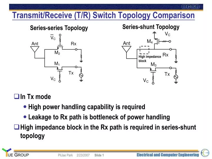
Transmit/Receive (T/R) Switch Topology Comparison. Series-shunt Topology. Series-series Topology. High impedance block. In Tx mode High power handling capability is required Leakage to Rx path is bottleneck of power handling

E N D
Transmit/Receive (T/R) Switch Topology Comparison Series-shunt Topology Series-series Topology High impedance block • In Tx mode • High power handling capability is required • Leakage to Rx path is bottleneck of power handling • High impedance block in the Rx path is required in series-shunt topology
Proposed T/R Switch • Series topology for Tx path, series/shunt LC tank for Rx path • For Tx mode, VC is high and L1, C1 forms parallel LC resonance tank • For Rx mode, VC is low and L1, C2 forms series LC resonance tank • Tx path has small area and high Power handling capability • Low IL input matching network can be absorbed into T/R switch In Triple Well
Inductive body bias MOS switch [2] Twin well MOS switch Proposed Floating Triple Well Tx Switch Advantages • Floating Triple well provides isolation to substrate • Prevent power loss through the substrate • Smaller area, wider bandwidth compared to the LC-tuned body bias technique Triple well MOS switch
Floating Triple well MOS Tx Switch Body Impedance • Floating wells has better substrate isolation than LC tank • Effective substrate impedance of high-Q LC tank is still less than 2 kW • Smaller area and wider bandwidth
Low IL Matching between T/R Switch and LNA • Rx path of switch incorporates the LNA input matching network to achieve lower IL and noise figure • Rx path IL of conventional T/R switch = IL of switch + IL of matching network
T/R Switch Design • Tx switch design for low IL and high isolation • Rx path design consideration with inductor Q • Simulation results of Tx and Rx path Rx path of T/R siwth Tx path of T/R siwth
Tx Switch Equivalent Circuit Model • Triple well NMOS equivalent circuit model Triple well NMOS cross-section view
2.0 dB 1.5 dB IL [dB] 1.0 dB 0.5 dB Insertion loss of Tx Switch • IL of on Tx switch is a function of Ron and Zj
15 dB 20 dB 25 dB 30 dB 35 dB Isolation Plot of Tx Switch • Isolation of off Tx switch is a function of C’sd and Zj
Tx Switch Transistor Sizing Tradeoff • Tradeoff between IL and isolation • width ↑ , IL ↓ and width ↓ , isolation ↑ • Green dotted line indicates transistor width meeting isolation • Blue line points out transistor width satisfying IL specification IL < 1 dB Isolation > 15 dB
Insertion Loss of Rx Path in the T/R Switch • High Q inductor is desirable for lower receive IL • IL is about 0.5 dB when Q is 10 L1 : 5nH, C1 : 950fF M1: 100u/120n
Isolation of between Tx Signal to Tx Path in the T/R Switch • High Q inductor is desirable for high isolation • Isolation is about 17 dB when Q is equal to 10 L1 : 5nH, C1 : 950fF M1: 100u/120n
Tx Path P1dB Simulation Results of T/R Switch • All switches are on in Tx mode • Pin at Tx port Pout at Ant port for Tx mode P1dB simulation • 31 dBm of P1dB is achieved
Rx Matching Simulation Results of T/R Switch • Matching between Ant and Rx is >20 dB at 2.3 GHz
Insertion Loss of T/R switch • Tx IL = 0.9 dB at 2.3 GHz • Rx IL = 1.3 dB at 2.3 GHz
Isolation Simulation Results • Tx port to Rx port isolation >23 dB at 2.3 GHz
T/R Switch Layout • 8-metal, 1-poly UMC 130-nm technology • Area of 500 μm x 500 μm including test pads • core 230 μm x180 μm 500 μm 500 μm
Performance Summary • Our design achieves the highest P1dB with comparable IL and isolation
References [1] “A 5GHz 108Mb/s 2x2 MIMO Transceiver with Fully Integrated +16dBm PAs in 90nm CMOS”, Palaskas, Y et al, Solid-State Circuits, 2006 IEEE International Conference, Feb. 6-9, 2006 Page(s):1420 - 1429 [2] “Integrated CMOS transmit-receive switch using LC-tuned substrate bias for 2.4-GHz and 5.2-GHz applications”, Talwalkar, N.A. et al, EEE Journal of Solid-state circuit, Volume 39, Issue 6, June 2004. [3] “21.5-dBm power-handling 5-GHz transmit/receive CMOS switch realized by voltage division effect of stacked transistor configuration with depletion-layer-extended transistors (DETs)”, Ohnakado, T. et al, Solid-State Circuits, IEEE Journal of Volume 39, Issue 4, April 2004 Page(s):577 – 584 [4] Mei-Chao Yeh; Zuo-Min Tsai; Ren-Chieh Liu; Lin, K.-Y.; Ying-Tang Chang; Huei Wang; “Design and analysis for a miniature CMOS SPDT switch using body-floating technique to improve power performance” Microwave Theory and Techniques, IEEE Transactions onVolume 54, Issue 1, Jan. 2006 Page(s):31 - 39 [5]Single-pole double-throw CMOS switches for 900-MHz and 2.4-GHz applications on p- silicon substrates, Heng-Jung Huang; O, K.K.; Solid-State Circuits, IEEE Journal of ,Volume 39, Issue 1, Jan. 2004 Page(s):35 – 41 [6]15-GHz fully integrated nMOS switches in a 0.13um CMOS process, Zhenbiao Li; O, K.K.; Solid-State Circuits, IEEE Journal of Volume 40, Issue 11, Nov. 2005 Page(s):2323 - 2328