Download
1 / 14
140 likes | 219 Views
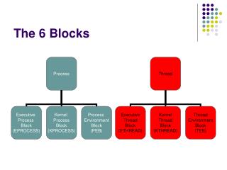
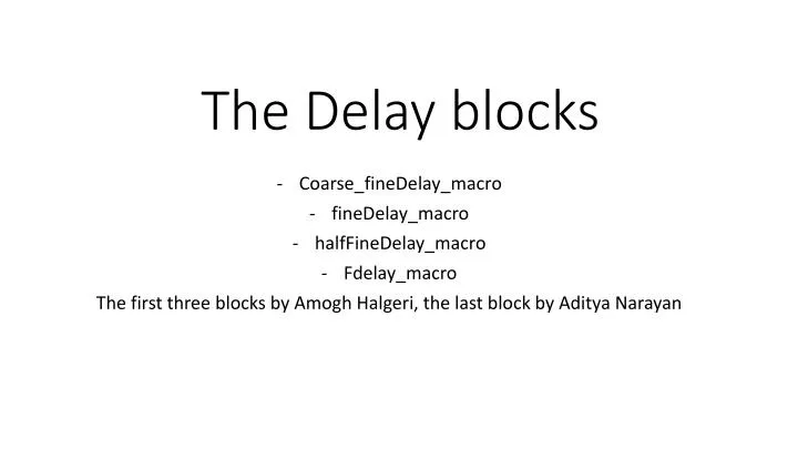
The Delay blocks. Coarse_fineDelay_macro fineDelay_macro halfFineDelay_macro Fdelay_macro The first three blocks by Amogh Halgeri, the last block by Aditya Narayan. Coarse_FineDelay_macro.

E N D
The Delay blocks Coarse_fineDelay_macro fineDelay_macro halfFineDelay_macro Fdelay_macro The first three blocks by Amogh Halgeri, the last block by Aditya Narayan
Coarse_FineDelay_macro • Four flip-flops to generate the coarse delay and fifteen delay blocks (each consisting of two DELAY_C’ elements) to generate fine delay • Coarse delay is a multiple of the clock cycle period, and fine delay is multiple of propagation time through delay blocks
Two input bits to select Coarse delay (sel_CoarseFineDelay[1:0]) among the four possible delays • Four bit input to select the fine delay (sel_fineDelay[3:0]) among the sixteen possible delays • The select bits are decoded using combinational logic to decide what delay is to be introduced
Spectre simulation of the extracted layout– slow process ; temperature - 500celcius • The minimum coarse delay – half a clock cycle. Clock is inverted to make it out of phase with incoming data signal. Thus the design is more robust (no race condition when data changes duty cycle from 35% to 65%, clkat 320 MHz, data at 40MHz) • The minimum fine delay – zero (Not passing through any of the delay blocks), delay through each DELAY_C element – 600 to 800 ps. Spectre simulation – Slow process and temperature of 500celcius
Average delay through a delay block– about 1.9 to 2 ns • This is the delay through two DELAY_C elements • Delay due to delay elements, wiring, the AO2222 cells and other combinational logic.
FineDelay_Macro The 30 delay cells and the decoder as depicted by cadence rtl compiler gui.
Same as the Coarse_fineDelay_macro block but without the flip-flops, and thus without the clock cycle delay. • Each AO2222 cell basically ‘and’s four pair of inputs and ‘or’sthe ‘and’ed outputs. • Four such cells used for selecting sixteen possible delays. • Each delay ‘block’ is serial combination of two DELAY_C cells. • Fifteen delay blocks are used, thus giving sixteen possible delays (one is zero - delay) • The four bit input ‘sel’ is decoded combinatorially before being used to select one of the possible sixteen delays. • The delay introduced by this combinational path is approximately 1.5 ns (simulated by spectre at 500 C , conservative analysis).
Spectre simulation of the extracted layout– slow process ; temperature - 500celcius • Average delay through a delay block– about 1.8 to 2.1 ns • This is the delay through two DELAY_C elements • Delay due to delay elements, wiring, the AO2222 cells and other combinational logic.
halfFine_Delay_macro The 15 delay cells and the decoder as depicted by cadence rtl compiler gui.
This block has fifteen delay ‘blocks’ each consisting of ONE DELAY_C cell • Apart from this difference, it is the same as fine delay macro • Delay control possible in smaller steps (0.8 ns instead 1.9 ns) • Makes use of AO2222 cells, and four bit input is decoded combinationally.
Fdelay_macro- Aditya Narayan • Selects one out of four input clocks and adds a delay to that clock specified by the four bit select input (sel_fdelay[3:0]). • Uses INVERTBAL_L cell instead of DELAY_C cell is the delay element. This provides a much smaller step delay (each ‘block’ has two cells and a rough delay of 0.1 ns) • Each inverter adds a delay of around 50-60ps and a Mux adds a delay of 200-350ps • Mux is used to select the clock to be transferred into the fdelay block (sel_FD [1:0] is the two bit select input) • Thus clocks from 80 MHz to 640 MHz can be transmitted out by introducing the required delay in them.
Block Diagram of FDelay_Macro, additional buffer and inverters added to maintain signal integrity
Each inverter adds a delay of around 50-60ps and a Mux adds a delay of 200-350ps. The additional inverters (apart from the delay cells) are used to provide greater load driving capacity.
Spectre simulations – for TT process A delay of 112.8 ps between two delay elements