Download
1 / 26
310 likes | 557 Views
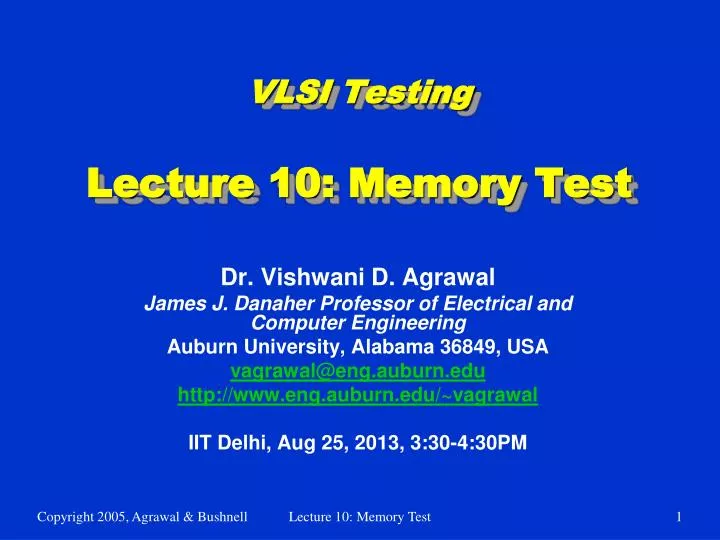
VLSI Testing Lecture 10: Memory Test. Dr. Vishwani D. Agrawal James J. Danaher Professor of Electrical and Computer Engineering Auburn University, Alabama 36849, USA vagrawal@eng.auburn.edu http://www.eng.auburn.edu/~vagrawal IIT Delhi, Aug 25, 2013, 3:30-4:30PM. Contents.

E N D
VLSI TestingLecture 10: Memory Test Dr. Vishwani D. Agrawal James J. Danaher Professor of Electrical and Computer Engineering Auburn University, Alabama 36849, USA vagrawal@eng.auburn.edu http://www.eng.auburn.edu/~vagrawal IIT Delhi, Aug 25, 2013, 3:30-4:30PM Lecture 10: Memory Test
Contents • Memory organization • Memory test complexity • Faults and fault models • MATS+ march test • Address Decoder faults • Summary • References Lecture 10: Memory Test
RAM Organization Lecture 10: Memory Test
Test Time in Seconds(Memory Cycle Time 60ns) Size Number of Test Algorithm Operations n2 18.3 hr 293.2 hr 4691.3 hr 75060.0 hr 1200959.9 hr 19215358.4 hr 76861433.7 hr n 0.06 0.25 1.01 4.03 16.11 64.43 128.9 n bits 1 Mb 4 Mb 16 Mb 64 Mb 256 Mb 1 Gb 2 Gb n × log2n 1.26 5.54 24.16 104.7 451.0 1932.8 3994.4 n3/2 64.5 515.4 1.2 hr 9.2 hr 73.3 hr 586.4 hr 1658.6 hr Lecture 10: Memory Test
SRAM Fault Modeling Examples SA0 SAF AF+SAF SA0 TF <↓/0> TF <↑/1> SCF <0;0> SCF <1;1> SA0 Lecture 10: Memory Test
DRAM Fault Modeling SA1+SCF SA1 AND Bridging Fault (ABF) ABF SA0 SCF ABF Lecture 10: Memory Test
SRAM Only Fault Models Faults found only in SRAM Open-circuited pull-up device Excessive bit line coupling capacitance Model DRF CF Lecture 10: Memory Test
DRAM Only Fault Models Model DRF SAF PSF CF PSF AF Faults only in DRAM Data retention fault (sleeping sickness) Refresh line stuck-at fault Bit-line voltage imbalance fault Coupling between word and bit line Single-ended bit-line voltage shift Precharge and decoder clock overlap Lecture 10: Memory Test
Reduced Functional Faults Fault Stuck-at fault Transition fault Coupling fault Neighborhood Pattern Sensitive fault* SAF TF CF NPSF * M. L. Bushnell and V. D. Agrawal, Essentials of Electronic Testing for Digital, Memory and Mixed-Signal VLSI Circuits, Springer, 2000, Chapter 9. Lecture 10: Memory Test
Stuck-at Faults • Test Condition: For each cell, read a 0 and a 1. • < /0> (< /1>) A A Lecture 10: Memory Test
Transition Faults • Cell fails to make a 0 → 1 or 1 → 0 transition. • Test Condition: Each cell must have an ↑ transition and a ↓ transition, and be read each time before making any further transitions. • <↑/0>, <↓/1> <↑/0>transition fault Lecture 10: Memory Test
Coupling Faults • Coupling Fault (CF): Transition in bit j (aggressor) causes unwanted change in bit i (victim) • 2-Coupling Fault: Involves 2 cells, special case of k-Coupling Fault • Must restrict k cells for practicality • Inversion (CFin)and Idempotent (CFid) Coupling Faults – special cases of 2-Coupling Faults • Bridging and State Coupling Faultsinvolve any number of cells • Dynamic Coupling Fault (CFdyn) – Read or write on j forces i to 0 or 1 Lecture 10: Memory Test
State Transition Diagram of Two Good Cells, i and j Lecture 10: Memory Test
State Transition Diagram for CFin < ↑ ; ↕ > Lecture 10: Memory Test
State Coupling Faults (SCF) • Aggressor cell or line j is in a given state y and that forces victim cell or line iinto state x • < 0;0 >, < 0;1 >, < 1;0 >, < 1;1 > Lecture 10: Memory Test
March Test Elements M0: { March element (w0) } for cell := 0 to n - 1 (or any other order) do write 0 to A [cell]; M1: { March element (r0, w1) } for cell := 0 to n - 1 do read A [cell]; { Expected value = 0} write 1 to A [cell]; M2: { March element (r1, w0) } for cell := n – 1 down to 0 do read A [cell]; { Expected value = 1 } write 0 to A [cell]; Lecture 10: Memory Test
March Tests Algorithm MATS MATS+ MATS++ MARCH X MARCH C- MARCH A MARCH Y MARCH B Description { (w0); (r0, w1); (r1) } { (w0); (r0, w1); (r1, w0) } { (w0); (r0, w1); (r1, w0, r0) } { (w0); (r0, w1); (r1, w0); (r0) } { (w0); (r0, w1); (r1, w0); (r0, w1); (r1, w0); (r0) } { (w0); (r0, w1, w0, w1); (r1, w0, w1); (r1, w0, w1, w0); (r0, w1, w0) } { (w0); (r0, w1, r1); (r1, w0, r0); (r0) } { (w0); (r0, w1, r1, w0, r0, w1); (r1, w0, w1); (r1, w0, w1, w0); (r0, w1, w0) } Lecture 10: Memory Test
Address Decoder Faults (ADFs) • Address decoding error assumptions: • Decoder does not become sequential • Same behavior during both read and write • Multiple ADFs must be tested for • Decoders can have CMOS stuck-open faults Lecture 10: Memory Test
Condition 1 2 March element (rx, …, w x ) (r x , …, wx) Theorem • A March test satisfying conditions 1 & 2 detects all address decoder faults. • ... Means any # of read or write operations • Before condition 1, must have wxelement • x can be 0 or 1, but must be consistent in test Lecture 10: Memory Test
March Test Fault Coverage SAF All All All All All All All All ADF Some All All All All All All All TF All All All All All All CF in All All All All All CF id All CF dyn All SCF All Algorithm MATS MATS+ MATS++ MARCH X MARCH C- MARCH A MARCH Y MARCH B Lecture 10: Memory Test
March Test Complexity Algorithm MATS MATS+ MATS++ MARCH X MARCH C- MARCH A MARCH Y MARCH B Complexity 4n 5n 6n 6n 10n 15n 8n 17n Lecture 10: Memory Test
MATS+ ExampleCell (2,1) SA0 Fault MATS+: { M0: (w0); M1: (r0, w1); M2: (r1, w0) } Lecture 10: Memory Test
MATS+ ExampleCell (2, 1) SA1 Fault MATS+: { M0: (w0); M1: (r0, w1); M2: (r1, w0) } Lecture 10: Memory Test
MATS+ ExampleMultiple AF: Addressed Cell Not Accessed; Data Written to Wrong Cell • Cell (2,1) is not addressable • Address (2,1) maps onto (3,1), and vice versa • Cannot write (2,1), read (2,1) gives random data MATS+: { M0: (w0); M1: (r0, w1); M2: (r1), w0 } Lecture 10: Memory Test
Memory Test Summary • Multiple fault models are essential • Combination of tests is essential: • March test – SRAM and DRAM • Other tests (see references on following slide): • NPSF – DRAM • DC parametric – SRAM and DRAM • AC parametric – SRAM and DRAM Lecture 10: Memory Test
References on Memory Test • R. D. Adams, High Performance Memory Testing, Boston: Springer, 2002. • M. L. Bushnell and V. D. Agrawal, Essentials of Electronic Testing for Digital, Memory and Mixed-Signal VLSI Circuits, Boston: Springer, 2000. • K. Chakraborty and P. Mazumder, Fault Tolerance and Reliability Techniques for High-Density Random-Access Memories, Upper Saddle River, New Jersey: Prentice Hall PTR, 2002. • K. Chakraborty and P. Mazumder, Testing and Testable Design of High-Density Random-Access Memories, Boston: Springer, 1996. • B. Prince, High Performance Memories, Revised Edition, Wiley, 1999. • A. K. Sharma, Semiconductor Memories: Testing Technology, and Reliability, Piscataway, New Jersey: IEEE Press, 1997. • A. J. van de Goor, Testing Semiconductor Memories, Chichester, UK: Wiley Interscience, 1991, reprinted by ComTex, Gouda, The Netherlands (http://ce.et.tudelft.nl/vdgoor/). Lecture 10: Memory Test