Download
1 / 22
220 likes | 224 Views
EECS 150 Spring 2007 . Checkpoint 0 - SDRAM 2/23/2007 Jeff Kalvass (Adapted From Greg Gibeling ). Welcome to Checkpoint 0. Agenda Why Checkpoint 0 is Important Checkpoint 0 Specs Theory of SDRAM SDRAM Init, Read, Write (timing diagrams) Designing the SDRAM controller. SDRAM

E N D
EECS 150 Spring 2007 Checkpoint 0 - SDRAM 2/23/2007 Jeff Kalvass (Adapted From Greg Gibeling)
Welcome to Checkpoint 0 • Agenda • Why Checkpoint 0 is Important • Checkpoint 0 Specs • Theory of SDRAM • SDRAM Init, Read, Write (timing diagrams) • Designing the SDRAM controller
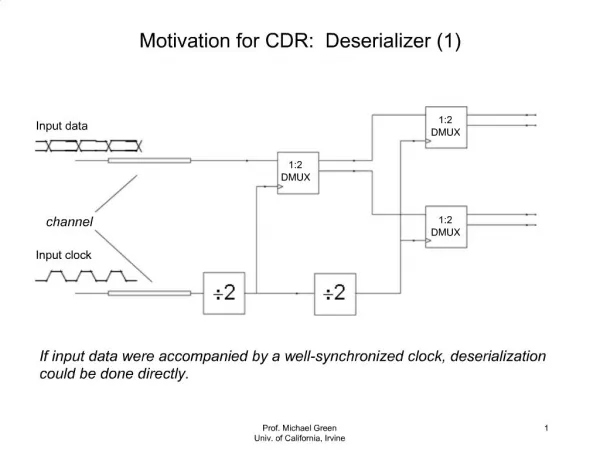
SDRAM (Checkpoint #0) Multiport Arbitration Motivation • Learn to configure external SDRAM • Write and read from external SDRAM • To use FIFOs as buffers • Design a memory controller • You will need this for the project
What is Checkpoint 0? (1) • Initialize and configure SDRAM • We provide 32-bit data generator • The black box we provide will handle all read and write requests • We will provide addressing scheme
What is Checkpoint 0 (2) • We provide data checker to compare what is read from SDRAM from what should have been written • Count the errors and display on LEDs
Theory of SDRAM (1) • SDRAM: Synchronous Dynamic RAM • Upside • Huge amounts of storage • Down side • Slow • May need refreshing every once in a while
Theory of SDRAM (2) • So to speed things up… • SDRAM handles bursts to read data as a group • Control requires precise timing • Issue sequences of commands • Timing must be matched with Data Sheet (more on this later)
Theory of SDRAM (3) • DRAM is BIG so we time mux address • Row Address • Column Address • Steps to Read/Write • Send Row Address • Send Column Address • Send/Get Data • Read the Data sheet for details
Theory of SDRAM (4) • SDRAM is a large FSM • Send it a command • Get a response • SDRAM Controller’s Job: • Send the right command signals • Ensure command sequences are timed correctly
SDRAM Specifications • See Spec at • http://www-inst.eecs.berkeley.edu/~cs150/sp07/Documents.php#Datasheets • Read the MT48LC16M16 Datasheet • Provides overview of commands and timing • You will need to become very familiar with initialization, reads, and writes
Write Timing • Memory chips are the -7E Models, and the clock is running at 27MHz
SDRAM Controller (1) • One Time • Initialization • Repeating • Read with auto-precharge • Write with auto-precharge • Auto-Refresh (only if idle for a long time)
SDRAM Controller (2) • Goal • Abstracts away the details of SDRAM • Accepts commands, produces responses • Deals with sending address in parts (row and then column) • Design Options • One large FSM, one small FSM with a counter, man small interacting FSMs, etc.
SDRAM Controller (3) • Design for the future! You will need it for your project • Tristate data line when reading!
FIFOs • Buffer to match two data rates • Great for data path clock domain crossings (we’ll talk about it later this semester)
The Checkpoint (1) • You have one week to complete this CP • Design Reviews next week at the beginning of your lab section (remember Lab 5 checkoff) • Bubble-and-arc diagram(s) required • Block Diagram highly recommended • Timing diagram required • Example: read and write
The Checkpoint (2) • Construction • Demo circuit on board for check-off • Remember you will be designing for CP1 concurrently • Groups of two – your lab #4/#5 partner • You must get checked off in the same lab section for the rest of the semester • Start designing today!
Any Questions? • Your friendly neighborhood lab TA is here • We want high completion for CP0, get help if you need it! • Sign-up sheet for partner/grading