Download
1 / 62
630 likes | 772 Views
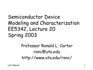
EE5342 – Semiconductor Device Modeling and Characterization Lecture 20 March 31, 2010. Professor Ronald L. Carter ronc@uta.edu http://www.uta.edu/ronc/. Schedule Change. Classes WILL be held on 4/5/10 4/7/10 Dr. Russell will be filling in

E N D
EE5342 – Semiconductor Device Modeling and CharacterizationLecture 20March 31, 2010 Professor Ronald L. Carter ronc@uta.edu http://www.uta.edu/ronc/
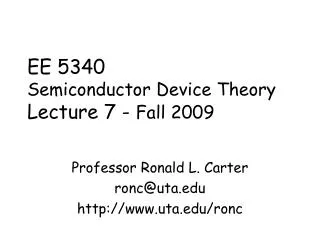
Schedule Change • Classes WILL be held on • 4/5/10 • 4/7/10 • Dr. Russell will be filling in • The previously scheduled make-up classes will be cancelled • 4/16/10 (Friday) • 4/23/10 (Friday) • Project 2 Test changed to W 4/28/10
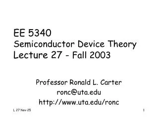
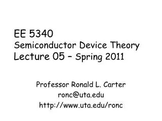
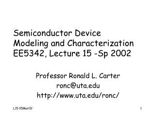
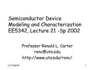
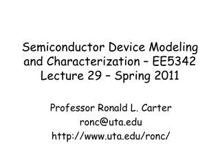
Inversion for p-SiVgate>VTh>VFB Vgate> VFB EOx,x> 0 e- e- e- e- e- Acceptors Depl Reg Vsub = 0
Inversion for p-SiVgate>VTh>VFB Fig 10.5*
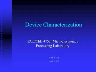
Approximation concept“Onset of Strong Inv” • OSI = Onset of Strong Inversion occurs when ns = Na = ppo and VG= VTh • Assume ns = 0 for VG< VTh • Assume xdepl = xd,max for VG = VTh and it doesn’t increase for VG > VTh • Cd,min = eSi/xd,max for VG > VTh • Assume ns > 0 for VG > VTh
MOS Bands at OSIp-substr = n-channel Fig 10.9*
Equivalent circuitabove OSI • Depl depth given by the maximum depl = xd,max = [2eSi|2fp|/(qNa)]1/2 • Depl cap, C’d,min = eSi/xd,max • Oxide cap, C’Ox = eOx/xOx • Net C is the series comb C’Ox C’d,min
n-substr accumulation (p-channel) Fig 10.7a*
n-substrate depletion(p-channel) Fig 10.7b*
n-substrate inversion(p-channel) Fig 10.7*
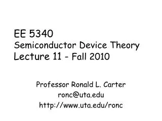
fms (V) Fig 10.15* NB (cm-3) Typical fms values
Flat band with oxidecharge (approx. scale) Al SiO2 p-Si +<--Vox-->- q(Vox) Ec,Ox q(ffp-cox) Ex q(fm-cox) Eg,ox~8eV Ec EFm EFi EFp q(VFB) Ev VFB= VG-VB, when Si bands are flat Ev
Inversion for p-SiVgate>VTh>VFB Vgate> VFB EOx,x> 0 e- e- e- e- e- Acceptors Depl Reg Vsub = 0
Approximation concept“Onset of Strong Inv” • OSI = Onset of Strong Inversion occurs when ns = Na = ppo and VG= VTh • Assume ns = 0 for VG< VTh • Assume xdepl = xd,max for VG = VTh and it doesn’t increase for VG > VTh • Cd,min = eSi/xd,max for VG > VTh • Assume ns > 0 for VG > VTh
Fig 10.9* qfp 2q|fp| xd,max MOS Bands at OSIp-substr = n-channel
Computing the D.R. W and Q at O.S.I. Ex Emax x
n-channel VT forVC = VB = 0 Fig 10.20*
Fully biased n-MOScapacitor VG Channel if VG > VT VS VD EOx,x> 0 e- e- e- e- e- e- n+ n+ p-substrate Vsub=VB Depl Reg Acceptors y 0 L
Fully biased MOScapacitor in inversion VG>VT Channel VS=VC VD=VC EOx,x> 0 e- e- e- e- e- e- n+ n+ p-substrate Vsub=VB Depl Reg Acceptors y 0 L
Flat band with oxidecharge (approx. scale) Al SiO2 p-Si +<--Vox-->- q(Vox) Ec,Ox q(ffp-cox) Ex q(fm-cox) Eg,ox~8eV Ec EFm EFi EFp q(VFB) Ev VFB= VG-VB, when Si bands are flat Ev
MOS energy bands atSi surface for n-channel Fig 8.10**
Ex Emax x Computing the D.R. W and Q at O.S.I.
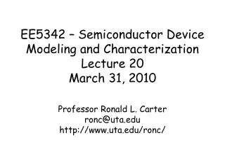
Q’d,max and xd,max forbiased MOS capacitor Fig 8.11** |Q’d,max|/q (cm-2) xd,max (microns)
n-channel VT forVC = VB = 0 Fig 10.20*
p-channel VT forVC = VB = 0 Fig 10.21*
Differential chargesfor low and high freq high freq. From Fig 10.27*
Ideal low-freqC-V relationship Fig 10.25*
Comparison of lowand high freq C-V Fig 10.28*
Effect of Q’ss onthe C-V relationship Fig 10.29*
n-channel enhancementMOSFET in ohmic region 0< VT< VG Channel VS = 0 0< VD< VDS,sat EOx,x> 0 e-e- e- e- e- n+ n+ Depl Reg p-substrate Acceptors VB < 0
Conductance ofinverted channel • Q’n = - C’Ox(VGC-VT) • n’s = C’Ox(VGC-VT)/q, (# inv elect/cm2) • The conductivity sn = (n’s/t) q mn • G = sn(Wt/L) = n’s q mn (W/L) = 1/R, so • I = V/R = dV/dR, dR = dL/(n’sqmnW)