Download
1 / 62
620 likes | 761 Views
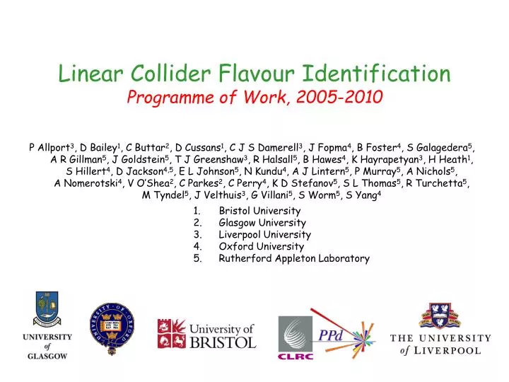
Linear Collider Flavour Identification Programme of Work, 2005-2010.

E N D
Linear Collider Flavour IdentificationProgramme of Work, 2005-2010 P Allport3, D Bailey1, C Buttar2, D Cussans1, C J S Damerell3, J Fopma4, B Foster4, S Galagedera5, A R Gillman5, J Goldstein5, T J Greenshaw3, R Halsall5, B Hawes4, K Hayrapetyan3, H Heath1, S Hillert4, D Jackson4,5, E L Johnson5, N Kundu4, A J Lintern5, P Murray5, A Nichols5, A Nomerotski4, V O’Shea2, C Parkes2, C Perry4, K D Stefanov5, S L Thomas5, R Turchetta5, M Tyndel5, J Velthuis3, G Villani5, S Worm5, S Yang4 • Bristol University • Glasgow University • Liverpool University • Oxford University • Rutherford Appleton Laboratory May 3, 2005
The LCFI collaboration has enjoyed 3 years of success in ILC vertex detector R&D The new five-year proposal moves us from Research into prototype detector Development Overall goal is to have a fully-functional and test-beam proven detector module, including sensors, readout, and mechanical support, ready in 2010. The challenge is to take bench-top devices and develop them into fully functioning modules Successful development will put us in the best possible position to build the ILC vertex detector New proposal includes 5 institutions 58 people, plus several students 7 new RA posts Linear Collider Flavour Identification – Goals May 3, 2005
LCFI Outline • 8 Work Packages: • WP1 Simulation and Physics Studies • WP2 Sensor Development • WP3 Readout and Drive Electronics • WP4 External Electronics • WP5 Integration and Testing • WP6 Vertex Detector Mechanical Studies • WP7 Test-beam and EMI Studies • WP8 Financial and Management May 3, 2005
ILC Physics Vertex Detector Design WP1 – Physics Studies • Physics studies are an essential part of the preparation • Drive the overall shape of the detector • Provide essential input for design concepts • Provide basis for the choice of various detector design parameters • Number, radii and length of modules • Arrangement of modules within barrel • Pixel size • Material budget • Quantify dependence of ILC physics on the vertex detector design • Tools required • Realistic Monte Carlo generator • Realistic simulation of the detector • Event reconstruction and analysis code May 3, 2005
WP1 – Vertex detector parameters to be optimised • Evaluating and optimising the physics performance requires attention to: • overall vertex detector design: radial positions (inner radius), length of modules, arrangement of modules in layers, overlap of modules (alignment), strength of B-field • the material budget: beam pipe, sensors, electronics, support structure (material at large cosq) • simulation of signals from the sensors: charge generation/collection, multiple scattering, effects of magnetic field • simulation of data processing and sparsification: signal and background hit densities, edge of acceptance • Programme of needed work falls into three categories: • Charge deposition, clustering, sparsification, track fitting (Task set 1.1) • Vertexing, track attachment, topological and angular dependence (Task set 1.2) • Impact on physics channels and physics quantities (Task set 1.3) Result will be a full understanding of the vertex detector and its capabilities “from MIPS to physics” May 3, 2005
Charge deposition, clustering, sparsification, track fitting Vertexing, track attachment, topological dependence Impact on physics quantities, individual physics channels dE/dx for 1 GeV p in 1 mm Si From MIPS to Physics (Task 1.1) The sensors studied are new devices; we need to model how they work. • We will need to develop understanding of: • Charge generation, propagation, and collection in new sensor types • Cluster finding, sparcification, fitting to tracks • Background effects and environment Provides feedback to sensor and electronics design May 3, 2005
Charge deposition, clustering, sparsification, track fitting Vertexing, track attachment, topological dependence Impact on physics quantities, individual physics channels c decay vertex b decay vertex e+ primary vertex e- From MIPS to Physics (Task 1.2) • Study factors affecting flavour identification and quark charge • Optimise flavour ID and extend quark charge determination to B0. • Examine effects of sensor failure. • Detector alignment procedures and effects of misalignments. • Polar angle dependence of flavour and charge identification. • Provides feedback to mechanical design; can shape overall detector design, e.g. additional layers, increased detector length vertex charge purity vs b-tag efficiency impact parameter resolution May 3, 2005
Charge deposition, clustering, sparsification, track fitting Vertexing, track attachment, topological dependence Impact on physics quantities, individual physics channels From MIPS to Physics (Task 1.3) • With complete simulation, study physics processes for which vertex detector is crucial, for example: • Higgs branching fractions, requires flavour ID. • Higgs self-coupling, requires flavour and charge ID. • Charm and bottom asymmetries, requires flavour and charge ID. Need to be prepared to react to discoveries at the LHC. Need to be prepared to show detector impact on physics. e+e- Zhh e+e- Zh May 3, 2005
WP1 – Physics Studies Deliverables • The main deliverables for WP1 are: • Studies that will guide optimisation of vertex detector designs. • Studies that will establish the physics potential for selected benchmark processes. • Evaluate the physics potential of the CCD, ISIS and FAPS vertex detector options, and provide code to the international ILC community. • Positions of responsibility in global ILC software development, in areas related to vertex detectors. • Major contributions to the detector Conceptual Design Reports, enabling LCFI to contribute strongly to the Technical Design Report for one of the global detector options. • Plans for simulation and physics studies • Extend current fast MC (SGV) to full MC simulation of effects in the vertex detector • Develop ‘high level reconstruction tools’ (vertexing, flavour tagging, Qvtx reconstruction) • Move increasingly to study of benchmark processes sensitive to vertex detector design May 3, 2005
337 ns 0.2 s Bunch Train x2820 0.95 ms Tracking and Timing Features at the Linear Collider What sort of tracking and vertexing is needed for the Linear Collider? • Vertex detectors for the Linear Collider will be precision devices • Need very thin, low mass detectors • No need for extreme radiation tolerance • Need high precision vertexing eg ~20 μm pixels • Can not simply recycle technologies used in LHC or elsewhere • High pixelization and readout implications • 109 pixels: must break long bunch trains into small bites (2820/20 = 141) • Read out detector many (ie 20) times during a train susceptible to pickup • …or store info for each bite and read out during long inter-train spaces Bunch Spacing May 3, 2005
Read out during the bunch train: Fast CCDs Development well underway Need to be fast (50 MHz) Proven track record at SLD Need to increase speed, size Miniaturise drive electronics Read out in the gaps: Storage sensors Store the hit information, readout between bunch trains (optimise for the ILC beam conditions) Readout speed requirements reduced (~1MHz) Can design to minimise sensitivity to electromagnetic interference Two sensor types under study; ISIS and FAPS WP2: Sensors for the ILC vertex detector ILC long bunch trains, ~109 pixels, relatively low occupancy May 3, 2005
Column Parallel CCD Readout time = N/Fout M N N “Classic CCD” Readout time NM/Fout WP2: Column Parallel CCDs • Fast Column-Parallel CCD’s (CPCCD) • CCD technology proven at SLD, but LC sensors must befaster, more rad-hard • Readout in parallel addresses speed concerns • CPCCD’s feature small pixels, can be thinned, large area, and are fast Bump-Bonded CPCCD + Readout CPCCD1 (e2v) May 3, 2005
Column Parallel CCD Readout time = N/Fout N Column-Parallel CCD development path • CPCCD Test Structures (Task 2.1: 2005 to 2006) • Lower clock amplitudes • Lower gate capacitance • Way to achieve improvements without designing new CCD • CPC3 (Task 2.2: 2007 to 2008) • Using the results from the CPCCD test structures • Large scale device • Hybrid driving system, first CCD with bump-bonded driver chip • Only one type of output circuits (voltage of charge) • CPC4 (Task 2.3: 2008 to 2009) • Size suitable for prototype ladders • Design clock speed achieved • Using second generation bump-bonded driver May 3, 2005
Column-Parallel CCD: CPCCD Test Structures Drive circuitry: “Clocking” the CPCCD sensors and achieving sufficient charge-transfer over the entire surface is one of the major challenges • Basic problem: 1 volt peak at 50 MHz across 40 nF 13 Amps • For CPC2-40 we expect 40 nF, ~2V peak • Study dedicated structures to minimise the load from the sensors on the drive circuitry: • Stepped nitride insulator under the polysilicon gates • Low-level implants under the polysilicon gates • Increasing the polyimide between metal bus layers • These improvements can be tested as “passenger” on existing wafer submissions at e2v technologies. Level 1 metal Polyimide Level 2 metal CPC2 Wafer ISIS1 Φ2Φ1 May 3, 2005
Can store charge for many crossings ISIS: In-situ storage image sensor Signal stored safely until bunch train passed– resistant to EMI Test device being built by e2v “Revolver” variant of ISIS Reduces number charge transfers Increases radiation hardness and flexibility No shortage of good ideas 20 μm 20 μm Storage Sensors – ISIS May 3, 2005
Storage Sensors – ISIS 4 5 Storage gate 3 6 Storage gate 2 RSEL OD RD RG 1 7 8 OS Output node to column load Output gate Transfer gate 8 Photogate 20 19 Charge generation Storage Transfer 18 17 Readback from gate 6 May 3, 2005
Reset transistor Source follower Row select transistor sense node (n+) reset gate row select to column load VDD storage pixel #1 storage pixel #20 output gate transfer gate photogate n+ buried channel (n) p+ well p+ shielding implant reflected charge Charge collection reflected charge substrate (p+) High resistivity epitaxial layer (p) Storage Sensors – ISIS • ISIS Sensor details: • CCD-like charge storage cells in CMOS technology • Processed on sensitive epi layer • p+ shielding implant forms reflective barrier (deep implant) • Dual oxide thickness possible • Overlapping poly gates not likely in CMOS, may not be needed • Basic structure shown below: May 3, 2005
Storage Sensors – ISIS • Standard CMOS process doesn’t allow overlapping polysilicon or two thicknesses of oxide. • Modify dopant profiles to produce deeper buried channel: single oxide? • Charge transfer is efficient, despite non-overlapping gates Sensor properties and design under study, looks promising Implant profile Charge transfer (ISE-TCAD simulation) May 3, 2005
20 μm 20 μm In-situ Storage Image Sensor development path • ISIS2 (Task 2.4: 2005 to 2006) • First CMOS-based ISIS • Range of test devices, linear and circular • Process development – 2 custom implants • Single devices and small scale arrays • ISIS3 (Task 2.5: 2007 to 2008) • Choosing the most promising ISIS architecture from ISIS2 • Larger pixel arrays, up to 20 mm 20 mm • Stitching tests • Readout chip bump-bonded or embedded • ISIS4 (Task 2.6: 2008 to 2009) • Full ladder-sized devices • Stitching perfected • Readout chip bump-bonded or embedded May 3, 2005
UK MAPS development MAPs: Monolithic active pixels Ongoing development for science by MI3 collaboration (Basic Technology) FAPS architecture Flexible active pixel sensors Adds pixel storage to MAPS Vreset Vdd Select Reset Out Storage Sensors – FAPS MAPS FAPS May 3, 2005
FAPS architecture Present design “proof of principle” test structure* Pixels 20x20 mm2, 3 metal layers, 10 storage cells First source measurements: 10 deep pipeline in each pixel Common mode noise subtraction (subtract Scell 1) S/Ncell between 15-17 With appropriate seed cut, inefficiencies <0.5% Storage Sensors – FAPS *(2-year PPARC funded programme to develop underpinning technology. Started June 2003) May 3, 2005
Flexible Active Pixel development path • FAPS1 (Task 2.7: 2006 to 2007) • Parametric test sensor • Several different architectures – variants of read and write amplifiers and storage cells • Several arrays of 6464 pixels • FAPS2 (Task 2.8: 2007 to 2008) • Choosing the most promising FAPS architecture • Larger pixel arrays, up to 20 mm 20 mm • Stitching tests • Readout chip bump-bonded or embedded • FAPS3 (Task 2.9: 2008 to 2009) • Full ladder-sized devices • Stitching perfected • Readout chip bump-bonded or embedded May 3, 2005
Storage Sensors – FAPS1 plans • Parametric test sensor • 64x64 identical pixels (at least) • Variants of write and read amplifiers and in storage cells • Will evaluate pixels in terms of • Noise • Signal • Radiation hardness • Readout speed • Optimisation is between • size of the pixel • readout speed • maximum amount of time available for readout • charge leakage Read/Write variations Memory cell variations May 3, 2005
WP3 – Readout Electronics • We need to read out 109 pixels • Order of magnitude more than either CMS, ATLAS pixels • Fortunately the pixels are sparsely populated per crossing (occupancy is low) • Readout electronics needs: • Digitisation: amplify and digitise signals from sensors • Filtering: filter out correlated noise • Sparsification: thresholds imposed and data sparsified so that only pixels containing information are kept • Clustering: neighbouring pixels saved • Output: output of multiplexed data Goal is to produce readout ASIC for full sensor width with these abilities May 3, 2005
WP3 – Scaling Effects in Readout ICs • First prototype: CPR0 • 1, 8 and 32-channel test structure • Designed to investigate multi-channel ADC • Results showed effects of cross-talk: worse for larger number of channels • First read-out IC: CPR1 Cross-talk problem solved, but new effects: • analogue amplifier matching • clock distribution for ADC switching • clocks for digital multiplexing Significant improvements in CPR2 as a result of understanding CPR1 test results • Conclusions • Scaling of mixed-signal ICs is non-trivial • Performance is difficult to simulate • Important to have several iterations • A robust design for CPR2 required insights from both CPR0 and CPR1 testing. May 3, 2005
CPR readout ASIC development plan • CPR2A (Task 3.2: 2006) • Same die size and bond-pad layout as CPR2 (5mm active width) • Bump-bond compatible with CPC2 • Improvements to analogue biasing • On-chip waveform generation, if necessary Benefits:fewer bond pads, simpler external control circuits, reduction of digital noise • CPR3 (Task 3.3: 2007) • 500 channels, 10mm width • Possible change of silicon technology (to match sensors) • Optimisation of circuitry and layout for low-voltage and 4-level metal Benefits: more compact digital blocks, verify that the CPR architecture is scalable to 10mm, possibly share costs with sensor production. • CPR4 (Task 3.4: 2008) • Full sized array :1000 channels, 20mm width • Layout optimised for high-speed, based on insights from CPR3 testing. Benefits:Layout compatible with detector ladder assembly May 3, 2005
WP3 – CPR Architectures • The block diagram for the readout IC could be virtually the same for all sensor options: • Front-end amplifiers • 5-bit ADC array and Gray code decoder • Digital back-end (sparsification, time-stamping, multiplexing) • There are minor differences in some blocks • Voltage amplifier for ISIS/FAPS, charge amplifier for CPCCD • Signal timing is different for ISIS/FAPS, compared to CPCCD • Many of the circuits developed for CPR could be re-used or adapted for ISIS/FAPS May 3, 2005
WP3 – Sensor-specific Details • There are differences between the outputs of CPCCD, ISIS, and FAPS. This makes it impracticable to implement a single readout IC. • CPCCD: charge output, typical signal ~2000 electrons • ISIS: charge storage, voltage output, ~5mV • FAPS: voltage storage, voltage output, ~50mV • There are also timing differences • CPCCD: 50MHz continuous readout during bunch train • ISIS/FAPS : slow ~1MHz readout after bunch train • It may be possible to combine the ICs for ISIS and FAPS using a switchable-gain voltage amplifier on the front-end. May 3, 2005
CPR-ISIS and CPR-FAPS details • CPR-ISIS3 and CPR-FAPS2 (Tasks 3.5, 3.7: 2007) • Dedicated ASIC, but drawing heavily from CPR2 • Not the same as CPR2 given timing differences • Bump-bond compatible with ISIS3 or FAPS2 • Possibility to include in sensor submissions, monolithic or stand-alone • CPR-ISIS4 and CPR-FAPS3 (Tasks 3.6, 3.8: 2008) • Full-scale ASIC for final module readout • Evolutionary development from previous CPR developments • Bump-bond compatible with ISIS4 or FAPS3 • Integration with sensor on one wafer desirable, but not assumed May 3, 2005
WP3 – Driver Design Issues for CPCCD • High Current • Problem supplying ~10A to driver IC (thick wires) • Solution may be capacitive storage (charged at low rate between bunch trains, discharged at high rate when CCD is clocked during bunch train) • Waveform shape and timing • The driver IC will provide a high degree of control over the waveform • Shape and timing of CCD clock could be fine tuned to match readout IC timing • Adjustable clock drive voltage (aim to minimise power, without degrading charge transfer efficiency) Driver circuit May 3, 2005
CPD Driver ASIC • CPD2 (Task 3.9: 2006) • Wire bonded to CPC2 • High current drive (~10A at 50MHz) • Large die size - important for power dissipation • Multiple bond pads, to minimise resistance and inductance • CPD3 (Task 3.10: 2007) • Bump bondable to CPC3 • Optimised for innermost detector layer • CPD4 (Task 3.11: 2008) • Bump bondable to CPC3/4 • Optimised for outer layers - higher current May 3, 2005
WP4 – External Electronics • Main objectives are to deliver • CPC and CPR test printed circuit boards • Storage sensor test printed circuit boards • CPD testboards, tests and transformer tests • Test benches/ladder electronics • Supplying test benches and their upgrades • Further firmware, LabVIEW and VME module design based on BVM2 and its daughterboards • Transformer drive for CPCCD • Testing air-core 16:1 PCB-based 1 cm2 • Requires modelling, test loads • Provides driver for CPC2 testing BVM2 base VME module May 3, 2005
CPC and CPR related test PCBs Five flavours (Tasks 4.2-4.7, 4.13-4.15) CPC standalone CPC with CPD clock drive CPC with transformer clock drive CPC with CPR CPR standalone Designed at Oxford Storage Sensor test PCBs Five flavours (Tasks 4.16-4.23) ISIS-2 standalone test boards 2 flavours CPR ISIS MB (CPR-ISIS + ISIS) CPR-ISIS standalone test board FAPS test boards Designed at RAL-ID WP4 Tasks CPC Clock drive: CPD test PCBs, CPD testing, transformer tests • Several activities (Tasks 4.8-4.12) • Simulation of devices, structures and drive chain. • Test board designs • Tests of devices, structures and drive chain. • Culminates in the clock drive solution for the CPC ladder. • Effort lead by Oxford May 3, 2005
Beam Test Electronics Beam test system (Task 4.24) Early involvement by Bristol in electronics designs will help testbeam Work Package Starting point is Oxford VME test system RAL will provide test of VME system Oxford and Bristol responsibility Off-ladder Electronics Designs for (Tasks 4.25, 4.26) For both the CPCCD and ISIS/FAPS Oxford focuses on CPCCD RAL works on ISIS/FAPS Oxford and RAL responsibility WP4 Tasks WP4 Management • Management (Task 4.27) • Leadership by Oxford May 3, 2005
WP5 – Integration and Testing • Objectives of WP5: • To gain a detailed understanding of the operation of the various sensors, their readout chips, drivers and associated electronics. • Understand bulk and surface radiation damage in the sensors. • Evaluate the parameters of the sensors for use as particle detectors. • Work package includes: • Testing of sensors, readout ASICs • Integration and Bump-bonding • Testing of integrated devices • Radiation Damage testing • Tests of sensors and electronics conducted at • RAL (PPD, ED/ID): CPCCD, ISIS, FAPS sensor testing, electronics testing • Glasgow: FAPS designs • Liverpool: Radiation Damage tests • Oxford: CPCCD and driver testing May 3, 2005
WP5 – Sensor Testing VME-based test stand • Sensor testing: CPCCD • CPC2+CPR2: stand-alone and bump-bonded evaluation (Task 5.1) • CPCCD test structures: dedicated PCBs, test CTI vs clock voltage (Task 5.2) • CPC3 and CPC4: devices will be fully bump-bonded w/ readout and driver. • Sensor testing: Storage Sensors • ISIS2 and FAPS1 testing: test devices on dedicated PCBs to determine sensor variant to use • ISIS and FAPS testing: dedicated PCB use same FPGA-based off-the-shelf test setups FPGA-based test board May 3, 2005
Bump-Bonding, Radiation Damage • Bump-bonding • Standard in semiconductor packaging… but not for small quantities, large devices, thinned devices, etc. • Necessary for dense, low-inductance connections • Primarily overseen by RAL, but Glasgow and Liverpool groups have experience • Radiation Damage studies • We need to characterise the process for resistance to radiation for any new vendor • Test bulk and surface damage for each sensor type • Look for charge transfer inefficiency in CPCCD, ISIS • Care and individual testing needed May 3, 2005
WP6 – Vertex Detector Mechanical Studies • Thin Ladder (module) construction Goals • 0.1 % X/X0 • Thinned silicon sensor • Uniformity over full length • Wire or Bump bondable • Robust under thermal cycling Work Package Goals: • Provide mechanical support for test beam studies (Tasks 6.1–6.2) • Two years of material and concept evaluation • Mechanical support technology (decision by March 2007) • detailed fixturing and prototype production 2007-2009 • Parallel global design and cooling thermal studies (Tasks 6.3–6.4) • support for above tasks • natural evolution into future real detector design May 3, 2005
WP6 – Mechanical (Tasks 6.1 and 6.2) • Materials and mechanical support technology under study • Carbon fibre, carbon foam, Silicon carbide foam, diamond, etc. • Reticulated vitreous carbon (RVC) foam; 3% relative density, 3.1mm = 0.05% X0 • Mechanical work located at • Bristol: materials research test stand, contact with Aerospace group • Oxford: silicon studies • Liverpool: simulation, ATLAS experience, materials studies • RAL: materials research, metrology, production development, liaison with contractors, fixturing, prototyping – considerable engineering support required materials studies support technologies metrology May 3, 2005
WP6 – Mechanical (Tasks 6.3 and 6.4) • Mounting schemes, layout, services, cooling etc must all be shown to be compatible with candidate technology • Large dependence on decisions in other work packages e.g. sensors, electronics • Mainly RAL, support from Oxford and Liverpool • Many mechanical challenges ahead • How to hold the ladders • Full detector layout • Thermal studies • How to cool the ladders • Stress analysis for candidate ladder support Many interesting mechanical challenges May 3, 2005
WP7 – Testbeams and Electromagnetic Interference WP7 Goals: • To understand the impact of the environment at the ILC on our sensors. • Beam induced RF had a serious impact on the SLD vertex detector. • The MDI panel of the world-wide study has identified EMI as one of the key issues to be addressed. • To test full-sized prototype detector modules in a Test-beam, including the study of: • Single hit efficiency • Resolution • Influence of high magnetic fields • Readout speed • Sparsification algorithms • Noise susceptibility We must ensure that we build a detector that works by selecting the most robust technology to deliver the best physics at the ILC May 3, 2005
WP7 – EMI Studies • Studies of Electromagnetic Interference • Study the effect of beam-related EMI in simple structures and on a system that is known to have suffered from electronic noise problems. • Understand the origin of the principal elements and structures of the ILC environment that allow leakage of RF/EMI from the beampipe, principally done through simulation in close contact with the group designing the final focus and beam delivery system and RF experts at Bristol. • Establish the sensitivity of our sensors to noise by injecting test signals directly into the sensor support electronics. • Working in collaboration with global community (ie SLAC, KEK). • Testing plan: • Develop instrumentation and make detailed measurements of the RF spectrum in test beams with different beam pipe configurations (SLAC). • We will model these different configurations and verify against the test-beam measurements. • We will develop a “bench-top” system to inject EMI. • Full-system test-beam with complete prototype ladder and readout chain May 3, 2005
Tasks for RA1: Simulations of Standard Model physics channels at the ILC Update of ZVTOP Study use of vertex information to improve jet finding Study Neural Net based flavour tagging Study vertex charge determination Study of novel support materials Preparation for test beam studies of CPC4, ISIS4 and FAPS3 Running of beam tests Analysis of test beam data Tasks for RA2: Radiation damage studies of the CPC2 and CPC3 Radiation damage studies of the ISIS2 and ISIS3 Radiation damage studies of the FAPS2 Simulation of radiation effects in the above devices using ISE-TCAD Development of analysis for beam tests of CPC4, ISIS4 and FAPS3 Running of beam tests Analysis of beam test data Tasks for RA3 Simulations of Higgs physics at the ILC Simulation of charge generation in sensors Simulation of charge collection in sensors Simulation of effects of cluster finding and sparsification algorithms Track fitting and production of track parameters and covariance matrices Tasks for RA4 Simulation of SUSY processes at the ILC Extension of vertex charge to neutral Bs using e.g. charge dipole Study of "recovery" algorithms for particular b and c hadron decay topologies Study of polar angle dependence of flavour tagging and vertex charge determination Study of alignment issues Integration of LCFI results into SGV, test and maintenance Tasks for RA5 Simulation of CPCCD performance using ISE-TCAD Tests of "passenger" CPCCDs Tests of CPC2, CPR1 and CPR2A (standalone and bump-bonded) Tests of CPC3, CPR3 and CPD3 (standalone and bump-bonded) Tests of CPC4, CPR4 and CPD4 (standalone and bump-bonded) Tasks for RA6 Simulation of ISIS performance using ISE-TCAD Tests of ISIS1 with light and X-ray signals Tests of the linear and revolver ISIS2 devices Tests of the ISIS3 and CPR-ISIS3 (standalone and bump-bonded) Tests of ISIS4/CPR-ISIS4 Tasks for RA7 Simulation of FAPS using ISE TCAD Tests of ISIS with RA6 Tests of the various FAPS1 devices Tests of the FAPS2 (standalone and bump-bonded) Tests of the FAPS3 (standalone and bump-bonded) Tasks for the New RAs May 3, 2005
Conclusions • 5-year development programme will best prepare us for the ILC May 3, 2005
LCFI Spokesman: T Greenshaw Project Manager: S Worm WP1 D Jackson WP2 K Stefanov WP3 S Thomas WP4 J Fopma WP5 J Velthuis WP6 J Goldstein WP7 D Cussans WP8 J Goldstein Bristol H Heath Glasgow C Buttar Liverpool T Greenshaw Oxford B Foster RAL S Worm WP8 – Financial and Management • The programme includes • 58 people, plus students, at 5 institutions • 7 new RA posts • £14.1 Million (£11.8M in non-rolling-grant) • £4.4M equipment (31%), the rest salaries • Management structure includes Spokesman, Project Manager, collaboration board, work package managers May 3, 2005
WP7 • Task 7.1 • EMI measuring instrumentation installed and working in FFTB (6 months) • Reproduce SLD VXD3 EMI problems in ESA test-beam (7 months) • Repeat EMI studies with R20 and modified beampipe/test structures (15 months) • Task 7.2 • Select RF modelling software and create initial models (6 months) • Implement understanding gained from EMI test-beams (9 months) • Predict RF/EMI environment of ILC interaction region (12 months) • Model susceptibility of CPCCD/ISIS sensors and electronics to RF/EMI (24 months) • Task 7.3 • Assemble toolkit to test susceptibility of sensors and readout electronics to injected noise (12 months) • Test available modules for susceptibility (24 months) • Task 7.4 • Assemble necessary infrastructure for first test-beam (30 months) • Data from first test-beam available (40 months) • Data from second test-beam available (50 months) • Analysis of test-beam data complete (60 months) May 3, 2005
Hardware May 3, 2005