Download
1 / 37
470 likes | 1.07k Views
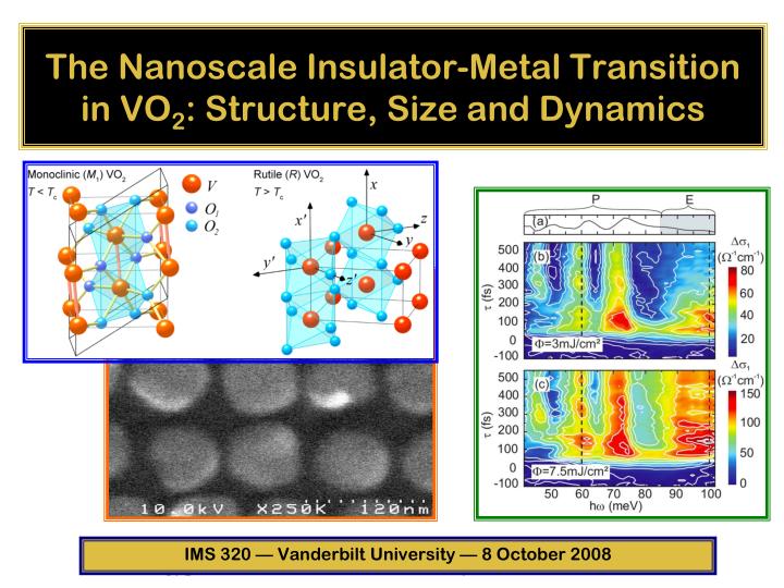
The Nanoscale Insulator-Metal Transition in VO 2 : Structure, Size and Dynamics. IMS 320 — Vanderbilt University — 8 October 2008. What you are about to hear …. Motivation: exploiting the metal-insulator transition Highly correlated solids and the phase transition

E N D
The Nanoscale Insulator-Metal Transition in VO2: Structure, Size and Dynamics IMS 320 — Vanderbilt University — 8 October 2008 Egyptian Materials Research Society
What you are about to hear … • Motivation: exploiting the metal-insulator transition • Highly correlated solids and the phase transition • Smart or functional nanoparticles • Nanoscale properties of metal oxides • Fabrication of VO2 nanoparticles • Optical properties of VO2 nanoparticles • Dynamics of the metal-insulator transition • What have we learned, and where are we going?
… strongly correlated electrons Itinerant electrons (Fermi liquid) CORRELATED ELECTRONS Tradeoff between hopping rate tij (kinetic energy) and Hubbard U (on-site Coulomb potential) Localized electrons (Mott insulator) Kotliar and Volllhardt, Physics Today, March 2004 for review of DMFT
VO2 metal-insulator transition • Morin, PRL, 1959 • First-order phase transition • Structural rearrangement • Gives D(conductivity)~104-105 • Large change in optical T, R • Can be triggered by laser • Entropy cost DS~1.6kB/V ion • Antiferromagnetic above TC Temperature dependence of resistivity in VO2 films Hysteresis loop; typical first order transition feature.
VOx focal-plane array bolometers • Vox bolometers are being developed for use in uncooled focal-plane IR detectors (8-14 µm). • Small size is critical, since it sets the spatial resolution of the focal-plane array given camera parameters • Little is known about the effects of granularity, stoichiometry and other materials parameters on detector performance (noise limits, etc.) • Photo credits: Raytheon Corporation
VO2: a martensitic phase transition • Structural phase transition alongside SMT: • T < Tc monoclinic • T > Tc rutile (tetragonal) • Monoclinic phase: • pairing and tilting of V cations • doubling of unit cell • One valence electron per V cation 3dcompound narrow bands e-e correlations • Which comes first, lattice change or SMT?
Mechanisms of metal-insulator transition • Dimerization of atoms unit-cell doubling • Opening of new band gap at Fermi level metal-insulator transition • Peierls deformation lowering of electronic energy (mostly near kF) vs. increase in elastic energy • Quasi-1D metals (e.g., VO2) susceptible to Peierls instability • Hubbard U: Coulomb repulsion between on-site electrons energy “penalty” for electron transport • Bandwidth W: determined by hopping between sites kinetic energy of electrons . • U ~ W itinerant vs. localized behavior Mott metal-insulator transition • Narrow-band systems (e.g., VO2) strong electron-electron correlations
First-order thermodynamics and hysteresis • First-order phase transformation: • discontinuous first derivatives of Gibbs free energy • entropy change latent heat of transformation • need for undercooling and overheating hysteresis around Tc • Avalanche-mediated transformation path: • athermal activation thermal fluctuations not operative • very recently observed in VO2 nanojunctions • Generic bistable potential linear tilt controlled by driving field h (e.g., |T – Tc|)
What you are about to hear … • Motivation: exploit the metal-insulator transition • Fabrication of VO2 nanoparticles • Ion implantation in bare SiO2 substrates • Pulsed laser deposition of V in O2 atmosphere • Fabricating nanoparticle arrays of VO2 • Optical properties of VO2 nanoparticles • Dynamics of the metal-insulator transition • What have we learned, where are we going?
nc-VO2 by ion implantation Ion acceleration Electrostatic Deflection (Rastering) Ion separation magnet Target Ion extraction O @ 55 keV, 3.0 x 10¹⁷ ions/cm2 V @ 150 keV, 1.5 x 10¹⁷ ions/cm2 Ion source Anneal 1000 ºC C-axis
Fabrication of Au::VO2 nanostructures • VO2 film by PLD • Stoichiometry by RBS • Switching by Topt(IR) • Morphology by SEM • Location by microscopy
Long anneal times • Hysteresis width and transition temperatures correlate with increasing nanocrystal size to Tanneal~450˚C
VO2vs V2O5 growth t=15 nm, T=450˚C, 250 mTorr O2, 40 min 2.00 µm 2.00 µm t=15 nm, T=550˚C, 250 mTorr O2, 40 min 1.00 µm 1.00 µm • VO2 NCs are hemispherical, implying no wetting of the Si substrate • X-ray data confirm that 550˚C anneal produces substantial V2O5 • Shape of high-temperature anneal NCs shows surface wetting
What you are about to hear … • Motivation: exploit the metal-insulator transition • Fabrication of VO2 nanoparticles • Optical properties of VO2 nanoparticles • Measuring the optical response of nanoparticles • Making valid comparisons for varying NP sizes • From characterization to modeling • Dynamics of the metal-insulator transition • What have we learned, where are we going?
Transmission experiments • Broadband white-light source • CCD spectrometer (0.3-1.2 µm) • Measure transmission vs temperature
Optical response vs size l=2.0 µm Increasing VO2 size Transmission Reff 37 nm 67 nm 80 nm 89 nm 87 nm b/a 1.3 1.9 2.7 3.2 3.5 Temperature (°C) V, 1.5 x 10¹⁷ ions/cm2 O, 3.0 x 10¹⁷ ions/cm2 Anneal in Ar 1000 ºC Nanoparticles by ion implantation Lopez et al., Phys. Rev. B (2002)
Nucleation and size-dependence of hysteresis Lopez et al., Phys. Rev. B65, 224113 (2002) • Energy barrier too high for homogeneous nucleation VO2 transition nucleates at heterogeneous “potent sites” • Availability F of potent sites depends on: • nanoparticle volume V • thermal driving “force” |T – Tc| • Smaller NPs larger driving force needed to transform wider hysteresis
Heterogeneous nucleation Density of defects is • IF : • The probability of finding an activated defect in a V is V • The probability of finding more than 1 defect in that V is negligible; • The probability of finding that defect is independent of other V’s; • Then Poisson statistics apply, and ... Defect probability is • Nucleation at special sites (structural or point defects?). • Not all defects have the same potency to nucleate the transition. • This potency must be thermally activated
Optical signature of nucleation T Switching Th Tc Temperature (ºC)
Size dependence of MIT Remember: Small is different! (“Small” depends on property.)
nc VO2 arrays • Remove VOx-coated PMMA by standard lift-off technique • Anneal in 250 mTorr O2 at 450C for up to 30 min. • RESULT: VO2 nanoarrays • Limited by PMMA thickness nc-VO2, typical disk diameter 60 nm, height variable, spacing variable. Rice University ECE Seminar
… and it is size-dependent 500 nm • Measured scattered (white) light, dispersed in CCD spectrometer • VO2 nanoparticles 120 nm diam • Lattice constant 280 nm • Resonance at 460 nm • Double hysteresis loop
An order-disorder transition Log(-ln(1-F) / V) Log gex (J/mole) • Note that the differing widths of the “bumps” parallels the differing Dgex dependence of heating and cooling transitions!
What you are about to hear … • Motivation: exploit the metal-insulator transition • Fabrication of VO2 nanoparticles • Optical properties of VO2 nanoparticles • Dynamics of the metal-insulator transition • Appearance of a metallic plasmon response • THz probe of AC conductivity • A model supporting recent theory • What have we learned, where are we going?
fs response of VO2 films and nc-VO2 • fs pump at 800 nm, fs IR probe • LSPR response as in adiabatic thermal phase transition Lopez et al., Applied Physics Letters (2004) M. Rini, R. Lopez, A Cavalleri et al., Optics Letters (2005)
Ultrabroadband THz study of VO2 Nd:YVO4, 18 W 4 MHz Ti:sapph amplifier tp = 12 fs; Ephot = 1.55 eV Opt. Lett. 28, 2118 (2003) VD1 tD VD2 T EOX WP balanced differential detector: ETHz(T), DETHz(T,tD) GaSe l/4 electro-optic analysis of both transmitted THz amplitude and phase i-InP, d = 230 nm VO2, d = 100 nm
What you are about to hear … • Motivation: exploit the metal-insulator transition • Fabrication of VO2 nanoparticles • Optical properties of VO2 nanoparticles • Dynamics of the metal-insulator transition • What have we learned, where are we going? • Novel geometries, stress and strain • Better materials and shorter pulses • Modeling the electric field effects
One more variation on geometry Probe laser Heating laser Glass VO2 film • SiO2 microspheres on glass by micropipette • Monolayer polycrystalline colloidal film • Microsphere diameter 1.54 µm in all cases • Laser heating and laser probing during MIT
Transmission measurements 100 nm on SiO2 100 nm film 140 nm on SiO2 140 nm film VO2 thin film samples VO2 film on SiO2 µspheres • Samples heated by ns Nd:YAG laser (532 nm) • Heating fluence ~ 10 mJ/cm2 • Transmission measured at 980 nm (cw diode) • Transmission on µsphere array increases!
So what is happening … and why? Tc~82˚C Tc~72˚C • The µsphere array is a diffraction grating … • … with light in both zeroth and first orders. • Measurement shows that MIT shifts intensity … • … from first to zeroth order in µsphere array. • It could be stress! • Epi-VO2 on TiO2 shows that Tc shifts higher with increasing stress (thinner films?)
Materials, geometries … nanophotonics • Oriented nanostructures • Better material(epi-VO2) • Exploit optical near field • Nonlinear optics (SHG, 3) • Other correlated materials?
What is to learn? • New materials and nanoscale structures • Materials: V2O3, VxCr1-xO2, WO3, … • Novel structures (e.g., arrays with curved surfaces, Konstanz) • Embedding materials designed for particular effects (e.g., NLO) • Ultrafast and angle-resolved studies of the effect: • Switching nonlinear effects using ultrashort laser pulses • Exploring the wavelength- and surface-dependence • What about the effect of the VO2 SPR (~1.3 µm)? • Ultrafast, THz and FIR studies • THz radiation could look at properties of the excited electron gas • FIR spectroscopy could help resolve controversial Raman results. • Early fs THz studies hint at MIT-related IR modes (Konstanz) • Nanoscale geometrical structure brings advantages of optical coherence to nanoscale differences!
The end … Picasso “Don Quixote” (in VO2) 2.31 µm Jae Suh René Lopez Matthew McMahon Eugene Donev “The legitimate purpose of research can only be, to make two questions grow where there was only one before.” [Thorsten Veblen] Thanks to the National Science Foundation and the United States Department of Energy for $$$!