Download
1 / 6
60 likes | 197 Views
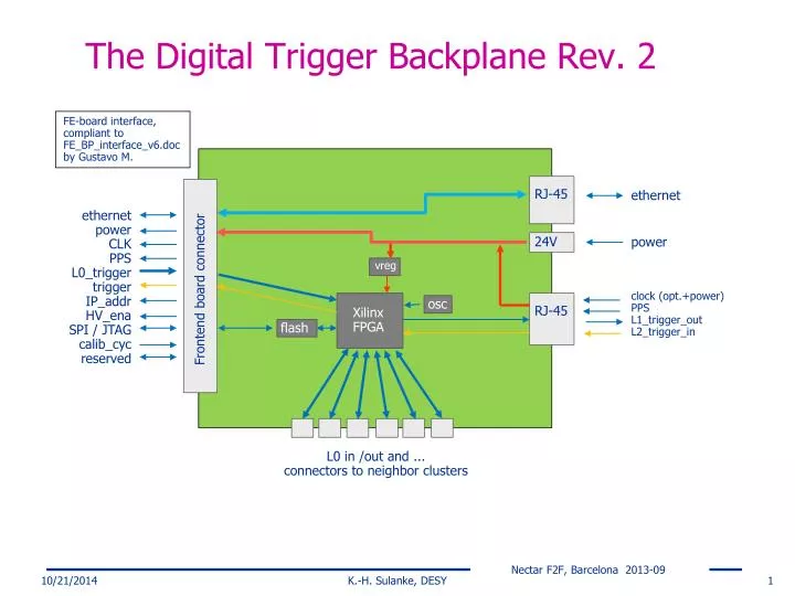
The Digital Trigger Backplane Rev. 2. FE-board interface, compliant to FE_BP_interface_v6.doc by Gustavo M. RJ-45. ethernet. Frontend board connector. ethernet power CLK PPS L0_trigger trigger IP_addr HV_ena SPI / JTAG calib_cyc reserved. 24V. power. vreg. clock (opt.+power)

E N D
The Digital Trigger Backplane Rev. 2 FE-board interface, compliant to FE_BP_interface_v6.doc by Gustavo M. RJ-45 ethernet Frontend board connector ethernet power CLK PPS L0_trigger trigger IP_addr HV_ena SPI / JTAG calib_cyc reserved 24V power vreg clock (opt.+power) PPS L1_trigger_out L2_trigger_in flash osc RJ-45 Xilinx FPGA flash L0 in /out and ... connectors to neighbor clusters 10/21/2014 K.-H. Sulanke, DESY 1
Digital Trigger Backplane, cont. FE-board Gigabit ethernet Hexadez. switches Clock_in PPS_in L1_out L2_in Xilinx JTAG conn. Xilinx FPGA 64 bit ID ROM local clock osc. 24V Power temp. sensor 50 pin flat cable FPGA PROM FE-board connectors DC-DC power supply 10/21/2014 K.-H. Sulanke, DESY 2
The DTB-FPGA‘s Functionality delay delay delay delay delay delay delay FPGA FPGA FPGA FPGA FPGA FPGA FPGA Xilinx Spartan 6 FPGA fanout to surrounding clusters from center cluster pix_[0][6..0] pix*_[0][4..0] calibrate STM progr. delays from surrounding clusters 37 pixel trigger fabric to L2_trigger board pix_[1][4..0] trigger pix_[6][4..0] clock PLL 10/21/2014 DESY 3
Three New Boards Developed Digital Trigger Backplane L0 Testboard L0 Mezzanine 10/21/2014 K.-H. Sulanke, DESY 4
The Cluster Service Board (CSB) vreg flash 16 x Cat5e cables RJ45 RJ45 RJ45 RJ45 RJ45 RJ45 RJ45 RJ45 RJ45 RJ45 RJ45 RJ45 RJ45 RJ45 RJ45 RJ45 Cur_mon 16 x switch Clock PPS L1_trigger L3_trigger Xilinx FPGA Or optional, including 24V 24V CLK PPS L2 L3 sdat JTAG Clock_PPS_24V GND L1_trigger L3_trigger Backplane connector 10/21/2014 K.-H. Sulanke, DESY 5
The Centralized Trigger Schema with L2 L2 also based on Xilinx-Spartan 6 FPGAs L2 is a crate, ~ 50 x 20 x 20 cm, ~ 11 kg 18 x CSB (Cluster Service Board) 1 x L2CB (L2 Controller Board) Ethernet interface Optical / electrical camera trigger output L2 DTB 24V (optional) L0_neighbor CSB L1 L2CB FEB 7 7 #01 L0 GPS_clock Sector_trig PMT #01 ethernet FPGA … L0_neighbor … L1 FPGA FEB FPGA #18 7 #16 7 L0 Camera_trig PMT FPGA PMT = Photomultiplier Tube FEB = Frontend Board DTB = Digital Trigger Backplane CSB = Cluster Service Board L2CB = L2 Controller Board 10/21/2014 K.-H. Sulanke, DESY 6