Download
1 / 2
20 likes | 171 Views
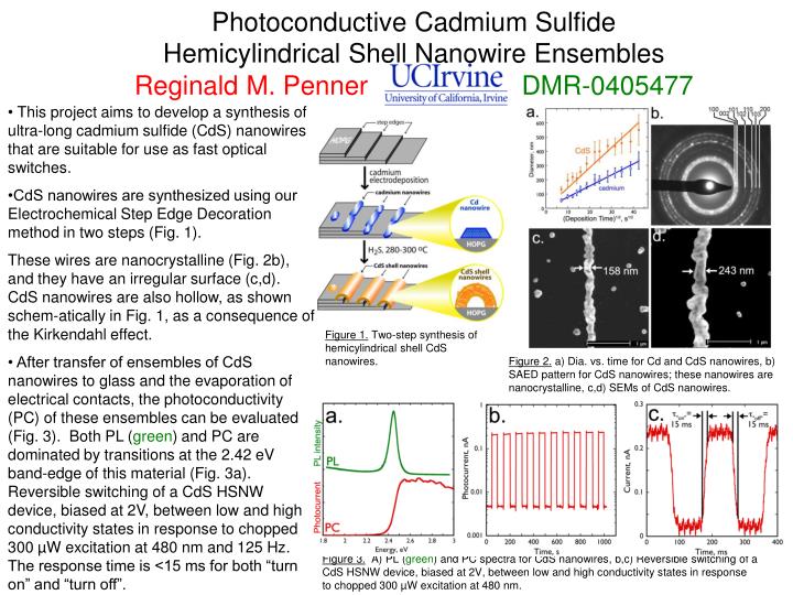
Photoconductive Cadmium Sulfide Hemicylindrical Shell Nanowire Ensembles Reginald M. Penner DMR-0405477. This project aims to develop a synthesis of ultra-long cadmium sulfide (CdS) nanowires that are suitable for use as fast optical switches.

E N D
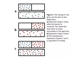
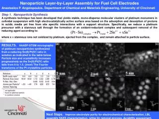
Photoconductive Cadmium Sulfide Hemicylindrical Shell Nanowire EnsemblesReginald M. Penner DMR-0405477 • This project aims to develop a synthesis of ultra-long cadmium sulfide (CdS) nanowires that are suitable for use as fast optical switches. • •CdS nanowires are synthesized using our Electrochemical Step Edge Decoration method in two steps (Fig. 1). • These wires are nanocrystalline (Fig. 2b), and they have an irregular surface (c,d). CdS nanowires are also hollow, as shown schem-atically in Fig. 1, as a consequence of the Kirkendahl effect. • • After transfer of ensembles of CdS nanowires to glass and the evaporation of electrical contacts, the photoconductivity (PC) of these ensembles can be evaluated (Fig. 3). Both PL (green) and PC are dominated by transitions at the 2.42 eV band-edge of this material (Fig. 3a). Reversible switching of a CdS HSNW device, biased at 2V, between low and high conductivity states in response to chopped 300 µW excitation at 480 nm and 125 Hz. The response time is <15 ms for both “turn on” and “turn off”. Figure 1. Two-step synthesis of hemicylindrical shell CdS nanowires. Figure 2. a) Dia. vs. time for Cd and CdS nanowires, b) SAED pattern for CdS nanowires; these nanowires are nanocrystalline, c,d) SEMs of CdS nanowires. Figure 3. A) PL (green) and PC spectra for CdS nanowires, b,c) Reversible switching of a CdS HSNW device, biased at 2V, between low and high conductivity states in response to chopped 300 µW excitation at 480 nm.
Outreach to Irvine High School StudentsReginald M. Penner DMR-0405477 In 2001, we established an outreach program in which high school students from two Irvine high schools, University and Sage Hill engaged in research projects in the Penner research group, under the direct supervision of a graduate student. These projects had a typical duration of 6 - 18 mos, and encompass at least one summer. All of these students prepared their results in poster form for presentation at the Orange County Science Fair, and several of these students proceeded to the California State Science Fair where they were awarded some of the top awards. Our program to date is summarized by the table shown at right, above. Presently, during summer 2005, we have two high school students (Johan Hong and Swetha Kambhampati), and a returning student (Albert Linden, now at UC Berkeley) working with us.