Download
1 / 36
370 likes | 384 Views
Peter Kr ü ger University of Nottingham. Atom chips. Microfabrication. Atom chip. Atom chips: concept. Quantum optics. Neutral atoms: weak interaction with the environment internal structure provides handles for manipulation. standard industrial process

E N D
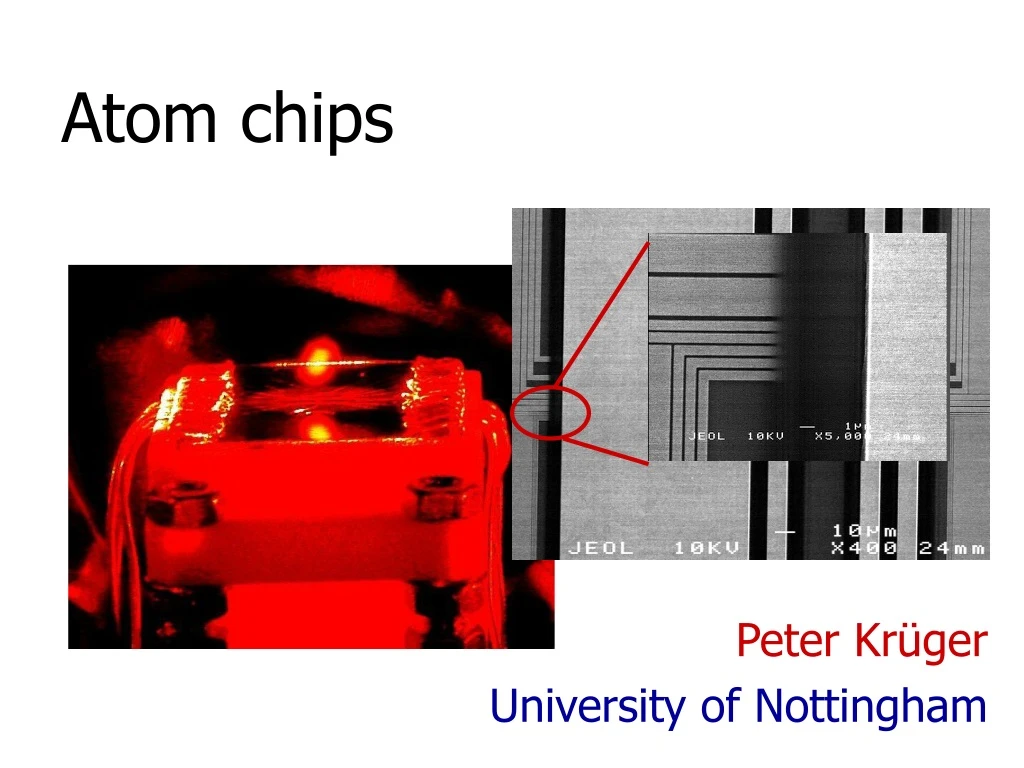
Peter Krüger University of Nottingham Atom chips
Microfabrication Atom chip Atom chips: concept Quantum optics • Neutral atoms: • weak interaction with the environment • internal structure provides handles for manipulation • standard industrial process • integration of different and complex components possible Integrated matter wave device for the control & manipulation of complex quantum systems
Degenerate quantum gases in low dimensions Quantum dynamics: single/few atoms, QIP Precision measure-ments: interferometry Surface probes/atom-surface interaction Atom chips: miniaturized atom optics • robust complex structures • steep trapping potentials at low currents & voltages • high trap gradients & frequencies • high aspect ratios (reduced dimensions) • non-trivial topologies • high tailoring resolution at low atom-surface distances
Outline • Atom chips: A toolbox for complex matter wave manipulation • Surface effects: coupling cold atoms – hot surfaces, rough potentials • Application: Chip based atom interferometry • Current routes: hybrid systems, low dimensional quantum gases in complex geometries
Manipulating potentials Tools & Techniques
Microscopic potentials • Magnetic interaction • current carrying wires: very versatile • micro magnets: strong quiet field • tight confinement • Electric interaction • additional degree of freedom • together with magnetic traps: • state dependent • Light fields • state independent guides and traps, • modified by electric and magnetic • fields from the microstructures • Integration with other techniques • cavity QED • nano-optics, nano electronics, MEMs
+ = Basic magnetic traps Superimpose field of current carrying wire with homogeneous bias field gives guiding potential Quadrupole minimum Bmin=0 U-trap: U-MOT Ioffe-Pritchard minimum (harmonic bottom) Bmin>0 Z-trap: Ev. cooling, BEC
Scaling laws Trap position (μm, G, mA) Confinement (gradient) w wire h Tolerated diss. heat Heat sink (substrate) Values of j (>107 A/cm2) possible for chip based wires, like superconductors
Side guide Omni directional guide duration of sequence: 250ms 5mm Luo, P. K., et al. Opt. Lett. 2004 Magnetic fields Folman, P. K., Cassettari, Hessmo, Maier, Schmiedmayer, PRL 2000
+ + + + + + + + + + + + HV electrodes side guide wire Electric fields Combined electric & magnetic interaction U(r) = gF mF µB B(r)–½ aE(r)2 • Electrostatic interaction • does not depend on mF • always attractive • Typical orders of magnitude (7Li) • UB [µK] 67 B [G] • UE [µK] 98 E2 [V/µm] Magneticside guide (1.6A / 44G) is modulated along axis of free movement by means of electric fields (300V) Periodic potentials (λ<1μm possible) P. K. et al., PRL 2003
Optical fields Arrays of microtraps: lattice with individual site addressability Birkl et al. • Standing wave formed by near-resonant red detuned (2-3nm) beam impinging the surface at an angle close to vertical • High transverse frequencies (>100 kHz) possible, single well loadable • 2d thermal gases and 2d BEC possible
Problem or virtue ? Surface effects
Setup Atom Chip 87Rb U-MOT • Cu-”U” replaces quadrupole coils for MOT: • Iw = 55 A, Bb= 8 G • >3 108 atoms in ~ 15s • > 105 atoms in BEC in various traps • BEC may be transferred or formed on site ‘H’: U/Z Broad U Wildermuth, P. K., Becker, Brajdic, Haupt, Kasper, Folman, Schmiedmayer, PRA (R) 2004
theory (layer) theory (bulk) Over-exponential rapid decay for small h (attractive surface pot.) See also Lin et al., PRL 2004 Surface effects: technical current noise • Coupling between hot surface (300K) and cold atoms (nK) via noisy currents • at Larmor frequency (spin flip losses) • trap frequency (heating) Theory by C. Henkel, predicts losses due to thermal current noise as a function of distance • data taken near flat current carrying wire • Lifetimes longer than predicted for bulk • Shorter than expected for layer • Residual technical noise
Thermal current noise Johnson noise in conductors leads to magnetic near field fluctuations • Rotation of bias field allows to place clouds close to conducting layer (z), but far from current carrying structure (d) • Separation between technical and thermal noise possible (in principle) • Large d result in low trapping frequencies, surface induced evaporation kicks in at higher z
Fragmented clouds near surfaces Tübingen (Cu) Sussex/London (Al) Jones et al., PRL 2003 Orsay (Au) Fortagh et al., PRA (R) 2002 MIT (Cu) Experiment: Estève et al., PRA 2004 Theory: Wang et al., PRL 2004 Leanhardt et al., PRL 2002
1μm 200nm 100nm Chip surfaces and fragmentation Wire imperfections cause non-straight current flow and potential roughness Groth, P. K. et al., APL 2004
Distance from wire (microns) Potential roughness characterization 1d limit TOF in spite of roughness, cloud stays continuous over 1 millimeter (width ~ 100 nm), aspect ratio ~10 000 P. K et al., PRA 2007
1d BEC as sensitive surface probe Two dimensional map of local disorder fields measured with BECs near a broad wire
Field maps & current reconstruction • 100μm wide wire • wire-atom distance 10μm (determines spatial resolution), may be smaller • paralleldisorder field components corresponding to current density components perpendicular to wire direction • sensitivity ΔB/B ~ 10-6 (10-13 eV) • reconstruction of high resolution current density map in conductors
Magnetic Field sensitivity: ΔB = γ ΔN / (ρ02z0) γ = 9.29·10-29 Tm3For87Rb atoms in the|F=2,mF=2> state Magnetic imaging: comparison ρ0=z0 =1μm a sensitivity of ΔB = 1nT is possible. By changing to a different atom with higher mass and/or by tuning the scattering length ascat to close to zero using a Feshbach resonance a significant increase in sensitivity can be achieved. Wildermuth, Hofferberth, Lesanovsky, Haller, Andersson, Groth, Bar-Joseph, P. K., Schmiedmayer, Nature 2005
measuring phases and phase correlations interferometrically Coherent manipulation
Time dependent beam splitter Electric beam splitter Interferometer potential Beam splitters
mF=+1/2 mF=+1/2 Ioffe field mF=-1/2 mF=-1/2 resonance condition shifts potential coupling term creates level repulsion the crossing is at a position where controlled by RF frequency ‘mF=+1/2 the levels are repelled by creating an effective Ioffe field, controlled by RF amplitude ‘mF=-1/2 New type of beam splitter Idea: use DC magnetic trap and couple different magnetic states with RF fields adiabatic potentials
Radio frequency beam splitter RF coupling term creates level repulsion • BECs can be split in separated double well over wide range (2-80 μm) • min. distance of wells given by trap ground state size • structures can be much larger • state dependent coupling Zobay, Garraway, PRL 2001 Experiments with thermal atoms: Colombe et al., Europhys. Lett. 2004 Relevance of polarization: Schumm et al., Nature Physics 2005
Fringes and coherence • split BECs expand and fall under gravity after trapping potential is turned off • information on contrast and phase of interference patterns • multiple realizations show constant phase relation of completely split (no tunneling) BECs Schumm, Hofferberth, Andersson, Wildermuth, Groth, Bar-Joseph, Schmiedmayer, P.K., Nature Physics 2005
Low dimensional gases and hybrid systems Current routes
1d Bose gases Transverse confinement strong enough, so that for 87Rb
100 µm Z wire transverse imaging 25 µm U wires I I 100μm 10 µm RF antenna 50 µm Z wire longitudinal imaging One dimensional gases on atom chips At ~50 microns from the wire very elongated (aspect ratios > 1000) smooth BECs can be formed 1d: μ ω
Momentum distribution: TOF Momentum distribution of the ground state ? μ ω Experiment: Measure density dependence of transverse cloud width after TOF expansion Fragmented cloud gives (almost) single shot measurement of large density span
1d time of flight: widths F. Gerbier, EPL 2005 Even in purely 1d, there is a mean field correction
Finite T: bimodal 1d clouds If the expansion for both a quasi-BEC and a thermal cloud is gaussian, how can they be distinguished (kT ~ ω) ? Discern the interferable fraction ! Fourier transform cold hot
t=0ms t=4ms t=8ms Time evolution coupled uncoupled Schumm et al., Nature Physics 2005 Hofferberth et al., Nature 2008
Interferometers and rings • Fully integrated wave guide interferometer: • RF amplitude controls splitting distance • A single RF current can provide varying RF amplitude if its width is adjusted Lesanovsky, Schumm, Hofferberth, Andersson, P. K., Schmiedmayer, PRA 2006 • Ring and torus geometries: • Static magnetic (quadrupole) rings can be modified with RF fields • Possibilities include homogeneous 2d torus surfaces, 1d rings, toroidal and poloidal stirring, 2 (coupled) rings, … Fernholz, Gerritsma, P.K., Spreeuw, PRA 2007
New group & experiments at Nottingham Non-trivial potentials, topologies Surface probes, atom-surface interaction/coupling Hybrid atom-semiconductor chips Chip based atom-light interfaces