Download
1 / 30
300 likes | 320 Views
Progress And Scientific Goals at ANL and UIUC. Klaus Attenkofer 50% growth; characterization; facility XSD Zikri Yusof 30% growth; facility HEP Bernhard Adams ~10% characterization XSD Igor Veryovkin ~10% characterization MSD Zeke Insepov ~20% Theory MCS

E N D
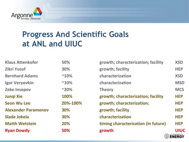
Progress And Scientific Goalsat ANL and UIUC Klaus Attenkofer 50% growth; characterization; facility XSD Zikri Yusof 30% growth; facility HEP Bernhard Adams ~10% characterization XSD Igor Veryovkin ~10% characterization MSD Zeke Insepov ~20% Theory MCS Junqi Xie 100% growth; characterization; facility HEP Seon Wu Lee 20%-100% growth; characterization; HEP Alexander Paramonov 30% growth; facility HEP Slade Jokela 30% characterization HEP Matth Wetstein 20% timing characterization (in future) HEP Ryan Dowdy 50% growth UIUC
The Design Concept of the Photocathode Itself • QE is defined by many factors: reflection losses, absorption probability, electron transport to surface, and electron emission • Cathode is heterogeneous structure: each layer influences the functionality of the others • All cathodes discussed are semiconductor cathodes: design principles can be applied to all three classes. Go to ”Insert (View) | Header and Footer" to add your organization, sponsor, meeting name here; then, click "Apply to All"
Theory Inspired Design of Devices Basic Energy Sciences (BES) supports fundamental research to understand, predict, and ultimately control matter and energy at the electronic, atomic, and molecular levels in order to provide the foundations for new energy technologies and to support DOE missions in energy, environment, and national security. Go to ”Insert (View) | Header and Footer" to add your organization, sponsor, meeting name here; then, click "Apply to All"
A Few General Comments about Cathodes of Interest • General properties: • All cathodes of interest are Semiconductors • All band gaps are between .6eV and 1.2eV (besides GaN). • The photo-electron: • 400nm photons have a energy of 3.1eV • All photo electrons are HOT-electrons • All cathodes are between 20nm-50nm thick (2-3 absorption length) • Consequences of cathode thickness: • Electron scattering on defects is not essential (may help to thermalize and randomize direction) • Interface and surface chemistry determines band banding (nearly not avoidable; also in the case of bi- and multi-alkali. • QE can be >100% Go to ”Insert (View) | Header and Footer" to add your organization, sponsor, meeting name here; then, click "Apply to All"
The Building Blocks at ANL Go to ”Insert (View) | Header and Footer" to add your organization, sponsor, meeting name here; then, click "Apply to All"
The Interface between Glass and Cathode Why is it important • Morphology and chemical composition (especially surface) have strong influence on growth-characteristics of cathode (crystallite/amorphous, grain boundaries,…) • Fermi-level will influence band-bending of the cathode • Large technological importance: • Less influence of cleaning procedure of glass-window • Less influence of glass composition • Conductivity allows higher count rate applications Glass: Fussed Silica or B33 ITO (ALD): 2 monolayer Al2O3 and 4.5nm ITO MgO: 5nm MgO layer applied with ALD Go to ”Insert (View) | Header and Footer" to add your organization, sponsor, meeting name here; then, click "Apply to All"
Optical Properties of Interface Layer Glass: Fussed Silica or B33 ITO (ALD): 2 monolayer Al2O3 and 4.5nm ITO • Silica and B33 show no indication for doping states (within “thermal resolution”) • Additional measurements (thoughts) will be necessary to determine if optical spectroscopy can trace surface states caused by cleaning procedure (increase of signal to noise figure by differential techniques) MgO: 5nm MgO layer applied with ALD Go to ”Insert (View) | Header and Footer" to add your organization, sponsor, meeting name here; then, click "Apply to All"
Optical Properties of Interface Layer Fussed Silica or B33 ITO • show no indication for distinct doping states (within “thermal resolution”) • Continuous increase indicates many doping levels with different energies (additional temperature dependent conductivity measurements will be necessary) MgO Go to ”Insert (View) | Header and Footer" to add your organization, sponsor, meeting name here; then, click "Apply to All"
Optical Properties of Interface Layer Fussed Silica or B33 • Bandgap:7.8eV (literature) • First increase around 5.5eV is according literature • Peak at 2.7eV is clear indication for doping level (O defect?) • After temper: absorbance is less!; peak disappears; onset sifts to low energy ITO MgO Go to ”Insert (View) | Header and Footer" to add your organization, sponsor, meeting name here; then, click "Apply to All"
Can We Understand the Optical Spectrum? • Energy levels of specific defects can be calculated (Insepov & Stegailov) • Theory includes relaxation effects! • Width and position of optical transition can be compared • Defect model helps to do the “right thing” (growth parameters) Phys. Rev. B 59, 5178–5188 (1999) J. Chem. Theory Comput., Vol. 4, No. 7, 2008 Go to ”Insert (View) | Header and Footer" to add your organization, sponsor, meeting name here; then, click "Apply to All"
The Model: What does that Mean for a Cathode • Will require more simulation and calculation • Basic understanding on influence on electric fields inside the device possible • Optical spectroscopy in combination with theory is an essential tool • Carrier densities will be needed (doping of the cathode) Go to ”Insert (View) | Header and Footer" to add your organization, sponsor, meeting name here; then, click "Apply to All"
Influences on Growth? • We are here on the starting point • Analytical tools (first applied to multialkali): • Exsitu AFM will determine the morphology • XAFS (X-ray Absorption Fine Structure): elemental composition and chemical bonding • Exsitu experiments: samples will be prepared by Burle-tool • In-situ setup with time resolved gracing incident techniques (depth sensitivity) • Gracing incidence scattering techniques • Ex-situ • In-situ • Depending on funding situation: These measurements can be compared with simulations Go to ”Insert (View) | Header and Footer" to add your organization, sponsor, meeting name here; then, click "Apply to All"
Surface X-ray Scattering Techniques Go to ”Insert (View) | Header and Footer" to add your organization, sponsor, meeting name here; then, click "Apply to All"
What can the Theory Do? • Microscopic model and calculation of the required energy levels of substrate • Growth simulation allows to develop microscopic model of growth • Prediction and guidance in growth parameters and surface manipulation Petrov, JVSTA 21 (2003) S117 Be aware: The cathode is only ~20nm thick! Go to ”Insert (View) | Header and Footer" to add your organization, sponsor, meeting name here; then, click "Apply to All"
M3Sb (M: K, Na, Cs)- Cathodes • “Good” knowledge of what is known: • Influence of gas-pressure on growth • Island growth-film growth transition at 12nm thickness • Vertical phase-segregation yield to band banding • Under-layer shifts cathode to red • PMT-cathodes are with high probability amorphous • Band structure calculations of different compounds • First PMT-like cathode made at Burle with Burle equipment • Clear plan how to come from a PMT-cathode (amorphous) to a transfer cathode • PMT-like cathodes will be used for first analytical tests (especially interlayer) • 4”x4” design for evaporator compatible with Burle equipment with “removable” cathode • Integration of Burle-concept into transfer-cathode fabrication center • The center will allow to take out samples which can be transferred to characterization centers (under UHV) Go to ”Insert (View) | Header and Footer" to add your organization, sponsor, meeting name here; then, click "Apply to All"
Short Glance on the Idea (more by Zikri) Surface Cleaning Interlayer Sb-layer (~15min at RT) Alkali treatment (~45min at ~160C) Seal at 50-80C Heating Chamber 350C over night SbPt on Pt/Mo wire Cs, K, Na sources Glass inset with pump and gas-manifold Glass inset with pump and gas-manifold One master plate will allow to process cathode and take 1cm diameter test samples Go to ”Insert (View) | Header and Footer" to add your organization, sponsor, meeting name here; then, click "Apply to All"
The Growth and Characterization Tools used for M3Sb (M: K, Na, Cs)- Cathodes • Growth: • Burle equipment (available in about 3month) • Exact recipe test • Engineering issues of evaporators • “Transfer-test” • Growth & Characterization Chamber (5-6 month) • Modifications of recipe • Cleaning procedure (ion/atomic source) • Base pressure influence on growth and functionality • Evaporation versus sputter • Sequential versus co-evaporation • Study of inter layer influence • Morphology • Electronic properties • Indirect structural properties • Production facility (9-12 month) • Homogeneity test • Recipe test Go to ”Insert (View) | Header and Footer" to add your organization, sponsor, meeting name here; then, click "Apply to All"
The Growth and Characterization Tools used for M3Sb (M: K, Na, Cs)- Cathodes • Characterization: • In-situ characterization of growth and characterization chamber • Optical spectroscopy (UV-VIS) with cryo-capability (200nm-1600nm) • Transmission and reflection • Angle dependence • Electrical characterization • QE • Photo-conductivity • Temperature dependent I-V curves • Lateral and transversal conductivity • Ex-situ (non vacuum) characterization • AFM • UV-VIS • Structural probes • Gracing incidence X-ray techniques (in collaboration with John Smedley (BNL) and APS) • First beamtime in December • Depth and lateral analysis by Igor (more by himself) Go to ”Insert (View) | Header and Footer" to add your organization, sponsor, meeting name here; then, click "Apply to All"
GaN Will be presented by Jim Buckley Go to ”Insert (View) | Header and Footer" to add your organization, sponsor, meeting name here; then, click "Apply to All"
GaAs: The Main Challenges • Wavelength optimization • Doping profile optimization • Minimizing dark-current • Transfer and bonding technology Go to ”Insert (View) | Header and Footer" to add your organization, sponsor, meeting name here; then, click "Apply to All"
Wavelength Optimization of Layer Thickness:The Optimization Criteria • Efficiency depends on • Probability to absorb photon • Probability to reach surface • (Probability to escape from surface is thickness independent) • Case GaAs (only an example) • Direct bandgap in IR (typical application) • Typical absorption length for IR: 1µm • Absorption length for 400nm: 30nm-100nm • Consequences: • Cathode has to be by a factor 10 thinner! • Photoelectron has defined kinetic energy • Thickness is thinner than mean free path-length • Crystallographic direction matters • Defect density, strain, …. at the interface between cathode and window matters! 413.2 nm 248nm 873 nm LAPPD: Second Collaboration Meeting 2010
What Happens in a 100nm Thick GaAs Cathode (400nm Photon) • Answer: NO • Creation of hot electron • Momentum in cathode plane!(electron will not reach surface if not scattered) • Result: • Low QE • Very slow • Solution: • Increasing scattering probability(can be done: tuning band structure to phonon distribution) • Better: creating internal electric field gradient • By doping gradient (what we have done) • Or by external electric Field. ? LAPPD: Second Collaboration Meeting 2010
The Doping Profile: The First Steps • Doping profile • Electric field distribution can be calculated by commercial simulation programs • Typical potential difference 0.1-0.2eV • Influence on timing behavior • Theoretical potential possible which allows transient time independent from absorption position! • Optimization possible even for very hard x-rays? LAPPD: Second Collaboration Meeting 2010
Is the Doping Profile Stable During Processing • Approach: • Minimizing process temperature • Using simulations to predict doping profile after processing • Calibrating simulations with selected samples using SIMS(Igor & Slade) • Status: • First simulations done by Zeke Insepov • In the process of creating SIMS measurements LAPPD: Second Collaboration Meeting 2010
The Emission Layer: The Standard Cleaning and Activation of GaAs As-rich Ga-rich e-J. Surf. Sci. Nanotech. Vol. 5 (2007) 80-88 LAPPD: Second Collaboration Meeting 2010
The Activation and Dark Current e-J. Surf. Sci. Nanotech. Vol. 5 (2007) 80-88 • Exact details of surface and Cs contribution determines electronic states of activation layer • Dark counts are highly effected by these details • Effects of morphology unknown • Long term stability depends on exact composition Phys. Rev. Lett. 81, 721–724 (1998) LAPPD: Second Collaboration Meeting 2010
Where We are Now? e-J. Surf. Sci. Nanotech. Vol. 5 (2007) 80-88 LAPPD: Second Collaboration Meeting 2010
The Transfer and Bonding Technology Grow thin layer of sacrificial AlGaAs Growth of photocathode, with layers inverted Deposition of intermediate bonding layers (i.e. SiO2, SixNx) Wafer bonded to a glass substrate predeposited bonding layers Bulk of substrate is etched/CMP away Sacrificial layer removed Photocathode ready for activation Glass substrate First test structured are made and characterized(roughness and shape errors (10x10mm2) Go to ”Insert (View) | Header and Footer" to add your organization, sponsor, meeting name here; then, click "Apply to All"
Bonding Apparatus Schematic 3x Guides IR Lamp Adjustable Height Metal Bracket Glass window Graphite Disk 3x Screw Shielding/Mirror Glass Block Go to ”Insert (View) | Header and Footer" to add your organization, sponsor, meeting name here; then, click "Apply to All"
Conclusion & Take-Home-Message • The selected cathode systems are: • M3Sb (M: K, Na, Cs)- Cathodes • GaAs (in collaboration with UIUC) • GaN (in collaboration and under lead of WashU) • All cathodes of interest follow the same physics principle • Similar band structure results in similar thickness requirements • Design principles can be transferred between • Materials science aspects are different for the three groups • Optical, electrical and many structural properties are known: clear program what has to be done • ANL is focused: • Creating proto-type production facility with most cost-efficient recipe • Creating the foundations that we will be able to cover the full spectral range after 2 years • Providing microscopic and macroscopic characterization tools • Providing state-of-the-art theory support utilizing collaborations • Communication with other institutions: • First test using the interlayer-study Go to ”Insert (View) | Header and Footer" to add your organization, sponsor, meeting name here; then, click "Apply to All"