Download

1 / 66
660 likes | 740 Views
Sampling front-ends Chips for Pico-second Timing with Micro-Channel Plate devices. Jean-Francois Genat University of Chicago Research Techniques Seminar Fermilab , Dec. 15 th 2009. With help from.

E N D
Sampling front-ends Chips for Pico-second Timing with Micro-Channel Plate devices Jean-Francois Genat University of Chicago Research Techniques Seminar Fermilab, Dec. 15th 2009
With help from John T. Anderson, MirceaBogdan, Dominique Breton, Gary Drake, Eric Delagnes, Henry J. Frisch, HerveGrabas, Mary K. Heintz, Edward May, Samuel Meehan, Eric Oberla, Larry L. Ruckman, Fukun Tang, Gary S. Varner, JaroslavVa’Vra and many others… Jean-Francois Genat, Fermilab December 15th 2009
Micro-Channel Plates The fastest devices to date • timing in the pico-second range • Fast Timing: Deep sub-micron CMOS technologies Pulse sampling at 1-10 GHz • large front-end at affordable power, room and cost • - Micro-channel Plate signals • Associated signal processing for pico-second timing • A 130nm CMOS sampling-digitizing ASIC Introduction Jean-Francois Genat, Fermilab December 15th 2009
Outline • Applications of Pico-second Timing • Micro-Channel Plate devices • Pico-second electronics and Waveform analysis • Sampling Electronics • Pico-second timing SCA in 130nm CMOS technology • Perspective Jean-Francois Genat, Fermilab December 15th 2009
10-100 Picosecond Time of Flight applicationsat HEP Colliders Non-TOF TOF Particle identification 1-100ps Time of Flight Henry Frisch Jean-Francois Genat, Fermilab December 15th 2009
10ns 10ns Particle ID from Waveform analysis Response to Pions to Muons Data from the Hadron Tile Calorimeter at LHC-ATLAS Pion signals have shorter lifetime: shorter signals and faster rise-time Sampled Waveform needed Jean-Francois Genat, Fermilab December 15th 2009
Lepton Flavor Physics Example: Deep Underground Science and Engineering Laboratory (DUSEL) detector Double b decay, Solar neutrinos, Gravitational waves 100% coverage and 3D photon vertex reconstruction. Need for >10,000 square meters at 100 psresolution ConstantinosMelachrinos (idea of Howard Nicholson) Henry Frisch Jean-Francois Genat, Fermilab December 15th 2009
100ps Time of Flight: Positron Emission Tomography [4] 10-100 Picosecond Time of Flight applicationsMedical Imaging Non-TOF TOF TOF JoelDx = c Dt/2 Dt=50ps, Dx=7.5mm arp Joel Karp Jean-Francois Genat, Fermilab December 15th 2009
A possible TOF PET detector Non-TOF TOF Henry Frisch Jean-Francois Genat, Fermilab December 15th 2009
Outline • Applications of Pico-second Timing • Micro-Channel Plate devices • Pico-second electronics and Waveform analysis • Sampling Electronics • Pico-second timing SCA in 130nm CMOS technology • Perspective Jean-Francois Genat, Fermilab December 15th 2009
Fast timing-Imaging Devices Multi-anodes PMTs Silicon-PMTs [10] Micro-Channel Plates [1] Dynodes Quenched Geiger in Silicon Micro-Pores Quantum Eff. 30% 90% 30% Collection Eff. 90% 70% 70% Rise-time 0.5-1ns 250ps50-500ps Timing resolution (1PE) 150ps 100ps20-30ps Pixel size 2x2mm250x50mm21.5x1.5mm2 Dark counts 1-10Hz 1-10MHz/pixel 1Hz-1 kHz/cm2 Dead time 5ns100-500ns 1ms Magnetic field no yes 15kG Radiation hardness 1kRad=noisex10 good (a-Si, Al2O3) Jean-Francois Genat, Fermilab December 15th 2009
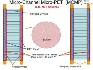
Timing (and Imaging) Devices Micro-Channel Plate Detectors[1-3] J. Vallerga Segmented Anodes anodes Timing Resolution: Single Photo-electronTimeTransit Spread: The thinner the device, the better the Timing resolution Aspect ratio (pore length/pore diameter) critical Jean-Francois Genat, Fermilab December 15th 2009
MCP Device Simulations: first gap (20-30ps total measured) Full device simulations: ValentinIvanov Zeke Insepov Jean-Francois Genat, Fermilab December 15th 2009
Two-micron space resolution usinganalog charge division technique High precision analog measurements. But integration time= 200ns ! Vernier Anodes geometry Jean-Francois Genat, Fermilab December 15th 2009
Micro-Channel Plate signals TTS= 10ps 11 mm diameter Micro-Channel Plate signal 2” x 2” Micro-Channel Plate signal Signal full bandwidth: 10 GHz Signal full bandwidth: 2 GHz Typical Timing resolution: Single Photoelectron Time Transit Spread: 10ps 30ps 2” x 2” imaging MCP (BURLE/PHOTONIS) From Photek Data taken at Argonne Jean-Francois Genat, Fermilab December 15th 2009
Timing resolution [5] Single Threshold Time spread proportional to 1/rise-time and noise Jean-Francois Genat, Fermilab December 15th 2009
MCP Signal in the frequency domain Fourier spectrum of a 2”x 2” MCP signal Noise as small as possible 2 GHz Slope as steep as possible Jean-Francois Genat, Fermilab December 15th 2009
t2, a2 Pico-second timing with delay lines: 2D position + time • Delay lines readout and pulse sampling provide - Fast timing (2-10ps) - One dimension with delay lines readout 100mm- 1mm Transverse dimension can be obtained from centroids Less electronics channels for large area sensors Pico-second electronics t1, a1 Pico-second electronics ½ (t1+ t2) = time v(t1-t2) = longitudinal position Sai ai /S ai = transverse position Jean-Francois Genat, Fermilab December 15th 2009
Delay Line readout Position resolution by fast timing 50 PEs Oscilloscope TDS6154C Tektronix 25 mm pore MCP signal at the output of a ceramic transmission line Laser 408nm, 50W, no amplification Jean-Francois Genat, Fermilab December 15th 2009
Delay Line readout Position resolution 158 PEs HV 2.3 kV 2.4 kV 2.5 kV 2.6 kV Std time diff 12.8ps 2.8ps 2.2 ps 1.95 ps Std position 640mm 140mm 110mm 97mm Oscilloscope TDS6154C Tektronix Jean-Francois Genat, Fermilab December 15th 2009
Delay Line readout Position resolution With Edward May and Eugene Yurtsev (Argonne) Jean-Francois Genat, Fermilab December 15th 2009
Delay Line readout Position resolution 158 Photo-Electrons Position resolution (velocity=8.25ps/mm) : 50PEs 4.26ps 213mm 158PEs 1.95ps 97mm Jean-Francois Genat, Fermilab December 15th 2009
Outline • Applications of Pico-second Timing • Micro-Channel Plate devices • Pico-second electronics and Waveform analysis • Sampling Electronics • Pico-second timing SCA in 130nm CMOS technology • Perspective Jean-Francois Genat, Fermilab December 15th 2009
Multi-threshold Pulse sampling and Waveform analysis Leading edge Constant-fraction Constant fraction Leading edge errors Extrapolated time Timing techniques ANALOG DIGITAL Sample, digitize, Fit to the known waveform Jean-Francois Genat, Fermilab December 15th 2009
Leading edge Constant-fraction Constant fraction Leading edge errors Constant fraction[6] Measure pulse amplitude: threshold at a given fraction a delayed version of the pulse 3-parameter (at least !) technique - Absolute Threshold - Fraction threshold - Delay Analog delay difficult to integrate (cable in most implementations) Jean-Francois Genat, Fermilab December 15th 2009
Multi-threshold: sample several times over thresholds Best results: - Number of thresholds 4-8 - Thresholds values equally spaced - Order of the fit: 2d order optimum Multi-threshold Extrapolated time Jean-Francois Genat, Fermilab December 15th 2009
Digital Waveform Analysis Fit to waveform and derivative templates Psec Timing and Charge Jean-Francois Genat, Fermilab December 15th 2009
Methods compared (simulation)[11] Time resolution vs Number of photo-electrons zoom Jean-Francois Genat, Fermilab December 15th 2009
Picosecond Digital Electronics for Micro-Channel Plate Detectors Fourier spectrum of a 2”x 2” MCP signal Noise as small as possible Store the full detector information as with a digital oscilloscope: - Quantization noise (LSB/√12) << Detector + electronics noise Sampling frequency > 2 x full Analog Bandwidth (Shannon-Nyquist) Ideal approach: Digitize on the fly, if the two above conditions can be fulfilled. If not, loss of precision due to A/D conversion and/or loss of timing information 2 GHz Slope as steep as possible Jean-Francois Genat, Fermilab December 15th 2009
Picosecond Digital Electronics for Micro-Channel Plate Detectors A/D state of the art: 8-bit 1GS/s 10-bit 300 MS/s 16-bit 160 MS/s Need at least 5 GS/s sampling rate, 10-12bit There is no ! Fast analog storage and slower digitization, if rate allows, or dead-time acceptable Apply the best timing algorithm suited to the detector, get the charge for free … ! Jean-Francois Genat, Fermilab December 15th 2009
Fast analog storage [7-9] Example: AnalogADC 5 GS/s analog storage, 8-ch 12-bit 80 MS/s (AD9222-80) Ok up to 2% occupancy - Internal Analog buffer or - Use other channels on-chip with a fast input multiplexer Jean-Francois Genat, Fermilab December 15th 2009
Assume: a typical noise at 1mV (detector+system) LSB set to 1mV for a 1V dynamic range (quantization noise 300mV), 50-200ps rise-time Fast timing: 10 bit, 2.5-10 GHz full analog bandwidth > 5-20 GS/s sampling rate Readout electronics Deep sub-micron CMOS ASICs: faster: larger analog bandwidth, sampling rate improved radiation hardness cheap, 1-10$/ch less dynamic range Sampled Micro-Channel Plate signals Jean-Francois Genat, Fermilab December 15th 2009
Outline • Applications of Pico-second Timing • Micro-Channel Plate devices • Pico-second electronics and Waveform analysis • Sampling Electronics • Pico-second timing SCA in 130nm CMOS technology • Perspective Jean-Francois Genat, Fermilab December 15th 2009
Fast Sampling Electronics • Integration in custom ASIC for large scale detectors ~ 104-6 channels, • Self or external trigger, • Low power, • Full digital (serial) interface, • High reliability and availability, • Low cost. Jean-Francois Genat, Fermilab December 15th 2009
Sampling Chips Sampling Bandwidth Dyn. range Depth PLL ADC Trigger Techno GS/s GHz bits bits G. Varner (Hawaii) [9] 6 1.0 10 1024 no 12 experience .25mm S. Ritt (PSI) [8] 6 .8 11.5 256 3.9ps no no .25mm D. Breton/E. Delagnes 2.5 .5 13.4 250 20ps no no .35mm (Orsay/Saclay) [7] ASIC Deep Sub-Micron ( < .13mm ) CMOS processes allow today: Sampling: 10-20 GHz Bandwidth: > 1.5 GHz Dyn. Range: 10bit Jean-Francois Genat, Fermilab December 15th 2009
Sampling Chips Survey Trade-off between analog resolution (10-14-bit) and timing (sampling rate 20 MHz-6 GHz) Our proposal: 130nm CMOS: optimize for timing resolution Jean-Francois Genat, Fermilab December 15th 2009
Existing ASICs: Labrador 3 [9] Gary Varner U-Hawaii CH1 6.4 ps RMS (4.5ps single) CH2 250nm CMOS After timing calibration Jean-Francois Genat, Fermilab December 15th 2009
Stefan Ritt Paul Scherrer Institute Switzerland • UMC 0.25 mm rad. hard • 9 chn. each 1024 bins,cascadable up to 8192 • Sampling speed 0.2 … 5 GS/s • Bandwidth 950 MHz • 17.5 mW/chn @ 2.5V • On-chip PLL stabilization • Readout speed usingext. ADC: 30 ns * nsamples • SNR: 69 dB calibrated • Aperture jitter: 4 ps at 5 GS/s calibrated Waveform Digitizing Chip DRS4 [8] No No 250nm CMOS Jean-Francois Genat, Fermilab December 15th 2009
The SAM (Swift Analog Memory) ASIC[7] D. Breton/E. Delagnes Orsay/Saclay • 2 differential channels • 256 cells/channel • BW > 450 MHz • Sampling Freq 400MHz->3.2GHz • High Readout Speed > 16 MHz • Smart Read pointer • Few externalsignals • Many modes configurable by a serial link. • Auto-configuration @ power on • AMS 0.35 µm => lowcost for medium size prod NIM A, Volume 567, Issue 1, p. 21-26, 2006 6000 ASICsmanufactured, tested and deliveredin Q2 2007 Jean-Francois Genat, Fermilab December 15th 2009
Sampling-Digitizing card using a CMOS ASIC S. Ritt PSI, Switzerland All these chips require a control FPGA for, at least, fine timing calibration purposes Jean-Francois Genat, Fermilab December 15th 2009
Outline • Applications of Pico-second Timing • Micro-Channel Plate devices • Pico-second electronics and Waveform analysis • Sampling Electronics • Pico-second timing SCA in 130nm CMOS technology • Perspective Jean-Francois Genat, Fermilab December 15th 2009
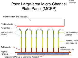
130nm CMOS Sampling ASIC 130nm CMOS is the best trade-off today between speed and dynamic range This chip is developed by U-Chicago and U-Hawaii It includes - 4 channels of full sampling (256 cells) - 1 channel of sampling cell to observe the sampling window Test structures: - Sampling cell, - ADC Comparator, - Ring Oscillator Jean-Francois Genat, Fermilab December 15th 2009
Sampling ASIC Prototype chip in 130nm CMOS technology (IBM 8RF-DM) 4-channel sampling, >10-15GSa/s 1-2 GHz analog bandwidth, 50 Ohms 40-80 MHz clock 256 cells (<100ps/cell, 12.5-25ns range) Free running delays (no PLL) Sampling window 500ps-2ns Dynamic range .8V Crosstalk <1% On-chip parallel 12-bit ADC (2 ms min conversion time) Free running delays (No PLL) Linearity < 1% on the full dynamic range Read clock up to 50 MHz (one cell/period, 22 ms total readout time) One reference channel (sampling window) 1.2V power supply Power < 40 mW/channel Process IBM 8RF-DM (130nm CMOS) 4 x 4 mm2 Chicago-Hawai’i Sent July 2009, received Oct 21st Jean-Francois Genat, Fermilab December 15th 2009
Block diagram Timing Generator Clock Channel # 0 (256 sampling caps + 12-b ADC) Ch 0 Read control Ch 1 Analog in Ch 2 Channel # 3 Ch 3 Digital out Calibration Channel #4 (Sampling window) Read Jean-Francois Genat, Fermilab December 15th 2009
Sequence of operations -1 Write: The timing generator runs continuously, outputs clock phases 100ps spaced. Each phase closes a write switch during one sampling window. 40 MHz Clk 100ps A/D converters Analog inputs Digital output Mux -2 A/D conversion after a trigger that opens all the write switches and starts all A/D conversions in parallel Data available after 2 ms (2GHz counters) -3 Read occurs after conversion (data can still be taken as in Phase 1) Jean-Francois Genat, Fermilab December 15th 2009
10 GS/s Timing Generator 100ps step delays Delay control voltages 256 cells 40 MHz clock 100ps 100ps100ps Sampling window control voltage To switched capacitor array Inverters delays used as time reference to be adjusted off-line for pico-second timing Jean-Francois Genat, Fermilab December 15th 2009
Timing Generator Voltage Controlled Delay Cell - 256 voltage controlleddelaycells of 100-200ps - 20-40 MHz clockpropagated Voltage Controlled Delay Cell Test structure: Ring Oscillator: Two delay cells + inverter Jean-Francois Genat, Fermilab December 15th 2009
rd wr wr Rin Cin Cin Cstorage Vout Vin Vin Vin Sampling Cell Principle “Write” state 3 dB analog bandwidth is 1/(2pRinCstorage) “Sampling window” Number of switches closed x sampling period Thermal kT/C switching noise = 250mV = one 12-bit ADC count Trade-off analog bandwidth - kT/C noise Jean-Francois Genat, Fermilab December 15th 2009
Rin Cstore Vin Analog bandwidth and Sampling window On chip: Rin is the resistance of the closed write switch Sampling window Sampling window = Number of switches closed at a time x sampling period Sampling Window10-3 = -log(10-3) x rise-time / 2.2= 1/ 3 dB Analog Bandwidth In practice, Rinand Cstore are minimum, but limited by the stray capacitor of the switch,the leakage current of the switch in the open state, and kT/C noise. Rin=1.5kW, Cstore= 70 fF 3dB Analog Bandwidth = 2 p RinC store= 1.5 GHz Sampling window 10-3 > 625ps = 7 samples at 10 GS/s Gary Varner Off chip: Inductance of the wire bonds and pad capacitance: Bump-bonding Jean-Francois Genat, Fermilab December 15th 2009
Sampling cell design Need a voltage buffer to read the small storage capacitor (70fF) The gate of the source follower transistor is part of the storage capacitor (40+30fF) Non-linearity < 8/1000 Jean-Francois Genat, Fermilab December 15th 2009