Download
1 / 23
230 likes | 373 Views
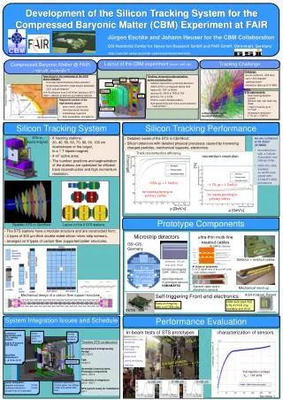
Status of the Silicon Tracking System. Johann M. Heuser, CBM Collaboration Meeting, GSI, 28.2.2008. News and update on Layout studies, realistic detector response Radiation environment Prototyping of detectors and components R&D Cooperations, Tasks. STS detector layout. 8 stations

E N D
Status of the Silicon Tracking System Johann M. Heuser, CBM Collaboration Meeting, GSI, 28.2.2008 • News and update on • Layout studies, realistic detector response • Radiation environment • Prototyping of detectors and components • R&D Cooperations, Tasks J.M. Heuser − Status of the Silicon Tracking System
STS detector layout 8 stations double-sided silicon micro-strip detectors, thickness 300mm Building block is a low-mass ladder structure Support made of carbon boxes Cables represented as capton boxes, thickness 200mm Readout electronics: thick layers of silicon and aluminium J.M. Heuser − Status of the Silicon Tracking System
Station layout Sectors: 6cm wide, 2 - 18 cm high Station 1 (R. Karabowicz) Station 8 About 1.2 million channels total.Occupancy reaches 5.7% in central Au+Au collisions at 25 AGeV. J.M. Heuser − Status of the Silicon Tracking System
Tracking results (R. Karabowicz) OLD SETUP WITH ADDITIONAL MATERIAL tracking eff. 93.8 % mom. resol. 1.7 % NEW SETUP WITHOUT ADDITIONAL MATERIAL tracking eff. 90.3 % mom. resol. 1.6 % OLD SETUP WITHOUT ADDITIONAL MATERIAL NEW SETUP WITH ADDITIONAL MATERIAL tracking eff. 87.9 % mom. resol. 1.6 % tracking eff. 96.18 % mom. resol. 1.3 % J.M. Heuser − Status of the Silicon Tracking System
Realistic detector response (I) Simple Event Display so far: single strips underneath Geant hits activated now: charge chared by several strips (R. Karabowicz) Size of plot [cm] Position in STS: X Y Z Sector view: Front strips in blue Back strips in green MC points in circles Reconstructed hits: stars Front strips’ ADC distribution Back strips’ ADC distribution J.M. Heuser − Status of the Silicon Tracking System
Realistic detector response (II) Problem: wide, overlapping clusters in the most upstream stations To be answered: Do we require pixel detectors in the first STS stations? J.M. Heuser − Status of the Silicon Tracking System
Tracking results - incl. clustering Clustering included tracking eff. 74.5 % mom. resol. 1.6 % Work in progress: DIGITIZER: TOO SIMPLE HIT FINDER: TOO SIMPLE Station 1 Station 8 (R. Karabowicz) J.M. Heuser − Status of the Silicon Tracking System
Radiation environment iFluka framework (D. Bertini) 1-MeV neutron equivalent fluences in CBM cave DPM (beam dump) UrQmd (interaction in target) J.M. Heuser − Status of the Silicon Tracking System
Radiation assessment in CBM (I) per min. bias UrQMD event, 25 AGeV (D. Bertini) J.M. Heuser − Status of the Silicon Tracking System
Radiation assessment in CBM (II) MDV+STS Scoring planes MUCH scoring planes J.M. Heuser − Status of the Silicon Tracking System
Neutron fluence in STS STS 5 STS 6 min. bias UrQMD @ 25 AGeV back scattering from MUCH absorber STS 7 STS 8 ~ 1 nequiv. per min. bias interaction Dose in 6 years of CBM running: ~ 3 1014 nequiv. Very Significant !! (D. Bertini) J.M. Heuser − Status of the Silicon Tracking System
Ionizing dose Station 1, z =30cm Calculated with GEANT for 6 years* of CBM running. *1 year = 2 months at 107 int/s (R. Karabowicz) comparable result with FLUKA Station 8, z =100cm Station 4, z =50cm J.M. Heuser − Status of the Silicon Tracking System
STS built from single-sided strip detectors • Why to study • Technology "radiation hard" • May be easier to construct a b a • Geometry composed of 28 stations • First station has vertical strips • Second station has stereo strips • 0.5 cm distance between stations. • Digitizer developed • Ideal hit finder combining strips belonging to one track. • Modified L1 tracking b First trials: (R. Karabowicz) (I. Kisel) Tracking efficiency ~ 80 % no advanced features included (e.g. no computing speed optimization) J.M. Heuser − Status of the Silicon Tracking System
Microstrip detector prototype CBM01, 8/2007 Test sensors 4" wafer, 285 µm Si Double-sided, single-metal, 256256 strips, orthogonal, 50(80) µm pitch, size: 1414 (22 22)mm2 CBM01B1 CBM01B2 Main sensor Double-sided, double-metal, 1024 strips per side, 50 µm pitch, 15º stereo angle, full-area sensitive, contacts at top + bottom edge, size: 5656 mm2 CBM01 Designed to explore CBM-specific connectivity J.M. Heuser − Status of the Silicon Tracking System
Towards 2nd design iteration CIS activity in frame of german BMWI project INNOWAT -“SPID“ L. Long and R. Rolf, CIS Test wafer to explore primarilyradiation tolerance Full detectors 7 pixel detectors; 18 strip detectors. Test structures: 3 Pad diodes, 4 Gate diodes, 6 PDTF, 2 SIMS, 2 SDM. poly silicon bias structures Process status 2/2008: First active implant finished. J.M. Heuser − Status of the Silicon Tracking System
1/C2 [pF-2] I [µA] I [µA] U [V] U [V] U[V] Characterization of CBM01 at CIS • IV and CV characterization of CBM01B1, CBM01B2, CBM02 (W. John et al.) • reported at CBM Meeting September 2007 J.M. Heuser − Status of the Silicon Tracking System
Find application in various activities of beginning detector module R&D Only currently available CBM-specific microstrip detectors. Very important for STS prototyping!! GSI: Test board (CBM01B2, preparation, report A. Lymanets) Test beam tracking module (planned) KINR Kiev: Pre-prototype module & CBM01B1 detector tests (electrical, diode laser, radioactive source) (report V. Pugatch) Kharkov/JINR: Test board with microcable fanout structure (planned) Cracow: n-XYTER-SUCIMA board with CBM01B2 (planned) + many new ideas around J.M. Heuser − Status of the Silicon Tracking System
Detector test board, GSI produced 2/2008 • test global detector characteristics • e.g. IV, CV • access both detector sides • contact a few strips for detailed measurements, including n-XYTER readout • do all this as quickly and as simple as possible to start work (A. Lymanets, J. Heuser) J.M. Heuser − Status of the Silicon Tracking System
Detector module pre-prototypes, KINR Kiev (V. Pugatch) CBM01-B1 detector: p-side on test board CBM01 detector, chip cable on carbon fibre support J.M. Heuser − Status of the Silicon Tracking System
I [µA] EStrip U [V] E Strip+1 CBM01 – first measurements at KINR Charge collection near surface Current-Voltage behaviour CBM01-B1 226 Ra from p-side, p-strips 5@6 EStrip Mapping of inter-strip charge charing with laser positioning system (V. Pugatch) µm J.M. Heuser − Status of the Silicon Tracking System HV = 50 V HV = 70 V
14 µm Al on 10 µm Kapton 55 cm long, 1024 lines, 100 µm pitch Readout cables, SE SRTIIE Kharkov (V. Borshchov et al.) 1024 strips50 µm pitch2 cm long first pre-prototypes produced Analog readout cable. J.M. Heuser − Status of the Silicon Tracking System
R&D cooperations, tasks ISTC project: “CBM Silicon Tracker“ (GSI, KRI St. Petersburg, MSU Moscow, IPHC Strasbourg) HadronPhysics2 I3 JRA: 9/2007Proposal: “Ultra-thin silicon tracking and vertex detection systems“ ... decision in 2008 ... CBM STS Consortium: 2008 - 2010 JINR-SINP-KRI-SPbSU-SESRITIIE-BTI-(IHEP)-GSI Finnland:FAIR member, in-kind contribution to CBM "single-sided rad-hard microstrip detectors" project under preparation To build and test a prototype(s) of the CBM STS Ladder GSI R&D cooperations: GSI-Kiev Inst. for Nucl. Research J.M. Heuser − Status of the Silicon Tracking System
Summary • STS still in conceptual design phase. • Progress with essential details, missing so far, is being made, including: • Realistic detector response (signal sharing, clusters) • Hit densities: - Strip technology in most upstream stations? - Are pixel detectors required? • Radiation study: How harsh are the operation conditions? • Deep consequences for the detector technologies and operating scenario. • Explore technologies: Double/single-sided strip detectors, AC/DC coupling... • Detector module concept: Very challenging design in mind, motivated by the low-mass requirement of our physics. Doable? • Risk management: Identify potential failures, redundant approaches, conservative and aggressive technical solutions. • Detector R&D: Essential. Becomes lively! Teams are forming. Preparations of test systems, test beams! • To aid this: Latest insights/results will be compiled in a technical document. J.M. Heuser − Status of the Silicon Tracking System