Download
1 / 42
440 likes | 596 Views
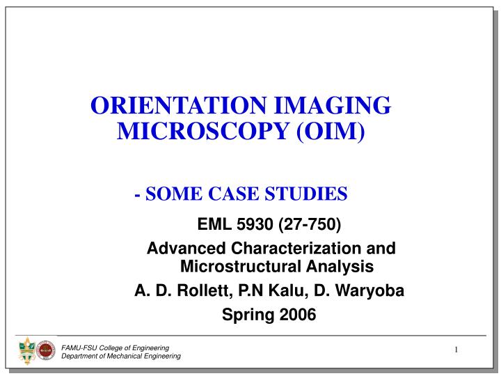
ORIENTATION IMAGING MICROSCOPY (OIM) - SOME CASE STUDIES. EML 5930 (27-750) Advanced Characterization and Microstructural Analysis A. D. Rollett, P.N Kalu, D. Waryoba Spring 2006. OUTLINE. REVIEW OF OIM CASE STUDIES

E N D
ORIENTATION IMAGING MICROSCOPY (OIM) - SOME CASE STUDIES EML 5930 (27-750) Advanced Characterization and Microstructural Analysis A. D. Rollett, P.N Kalu, D. Waryoba Spring 2006
OUTLINE • REVIEW OF OIM • CASE STUDIES • Development of Polishing Technique For OIM Study of Heavily Deformed OFHC Copper • Recrystallization in Heavily Deformed OFHC Copper • Heavily Deformed Cu-Ag • Deformed and Annealed OFHC Copper • Deformed and Annealed Cu-Nb • Other Examples
INTRODCUTION TO OIM - Diffraction • Diffraction of inelastically scattered electrons by lattice planes (hkl) according to Bragg’s law: • Sections of a pair of Kossel cones form a pair of parallel straight Kikuchi lines on the flat phosphor screen. • For maximum intensity, the specimen surface is steeply tilted at an angle of 20°-30° from grazing incidence.
TECHNIQUE DEVELOPMENT • EBSPs from a sample prepared by standard metallographic technique: Polished (a) OIM grain boundary map and (b) EBSD patterns
(b) (a) TECHNIQUE DEVELOPMENT • EBSPs from a sample prepared by standard metallographic technique: Polished + etched (a) OIM grain boundary map and (b) EBSD patterns
(b) (a) TECHNIQUE DEVELOPMENT • EBSPs from a sample prepared by Novel technique - Polished + Etched + Polished (a) OIM grain boundary map and (b) EBSD patterns
Confidence Index Image Quality Confidence Index Image Quality
IPF of wire drawn OFHC copper deformed to = 3.2, obtained via (a) OIM and (b) X-ray diffraction techniques TECHNIQUE DEVELOPMENT • CONCLUSIONS • Polishing by the novel technique, which consists of polishing+etching+polishing, produced high quality EBSPs leading to excellent OIM image. • IPF from OIM were consistent with the IPF from X-ray diffraction
Optical micrograph showing microstructure after deformation to = 3.2, = 405 MPa. Arrows show pockets of recrystallized grains. Optical micrograph showing microstructure after deformation to = 1.3, = 392 MPa. No recrystallization Rex in HEAVILY DEFORMED OFHC COPPER • Microstructure
(a) (b) U W V DD Y X Rex in HEAVILY DEFORMED OFHC COPPER OIM map showing grain orientations at (a) p = 2.3, UTS = 411.5 MPa, and (b) p = 3.2, UTS = 405 MPa. The lines represent high angle boundaries, with misorientation > 15o.
<112>54° {-265}<-12 22 –7> <213>75° {-3 11 6}<-65-2> <-4-13>45° {1 11 18}<7 29 2> 1 <313>85° {184}<-12 17 2> <12-6>40° {-4-19}<-46-3> <1-21>26° {-212}<-34-5> <1-1-3>48° {-8713}<25-3> 13 <-1-15>56° {-2 14 23}<13 11 –1> <-211>63° {3-4 11}<6 10 3> <144>60° {-6 13 5}<-24-2> <-210>36° <1-1-1>64° {-201}<23-8> <112>65° <-1-12>60° {198}<12 23 2> <2-1-2>52° 10 <2-1-1>65° <-1-12>60° 11 12 <-210>32° <2-1-3>55° <313>66° <4-2-1>42° <133>65°
Rex in HEAVILY DEFORMED OFHC COPPER OIM map showing grain orientations after deformation to p = 3.6, UTS = 390.5 MPa.
OIM maps of a heavily drawn Cu ( = 3.2) showing regions of shear bands. Shaded IQ map of a heavily drawn Cu ( = 3.2) showing regions of shear bands. 1 2 Sh/B in HEAVILY DEFORMED OFHC COPPER
Rex in HEAVILY DEFORMED OFHC COPPER • CONCLUSION • Three regions were identified: • Low processing strain < 2.5: No recrystallization, elongated structure. • Intermediate strain 2.5 < < 3.2: Nucleation of recrystallization, shear bands formation. Shear bands occurred in grains with S{123}<634> orientation, and were inclined at 54° to the drawing direction. Their misorientation was between 5°s10°. • High strain > 3.2: Extended recrystallization, recrystallized grains were mainly of Cube {001}<100> and S{123}<624> orientations. • OIM proved to be a viable tool in the study of heavily deformed materials.
Optical micrograph of a heavily drawn CuAg ( = 3.2) showing regions of shear bands. Shaded IQ map of a heavily drawn CuAg ( = 3.2) showing regions of shear bands. HEAVILY DEFORMED CuAg
2 1 OIM maps of a heavily drawn CuAg ( = 3.18) showing regions of shear bands. The Grain boundaries were constructed with a misorientation criteria of 15°. HEAVILY DEFORMED Cu-Ag
ANNEALED OFHC COPPER - Microstructure (a) Optical micrograph of annealed Cu, p = 3.1, 750°C (a) Optical micrograph of annealed Cu, p = 3.1, 350°C
ANNEALED OFHC COPPER OIM tiled IPF map showing grain orientations for Cu wire drawn to a strain of 3.1 and annealed at 250°C for 1 hr.
ANNEALED OFHC COPPER OIM tiled IPF map showing grain orientations for Cu wire drawn to a strain of 3.1 and annealed at 300°C for 1 hr.
ANNEALED OFHC COPPER OIM tiled IPF map showing grain orientations for Cu wire drawn to a strain of 3.1 and annealed at 500°C for 1 hr.
ANNEALED OFHC COPPER OIM tiled IPF map showing grain orientations for Cu wire drawn to a strain of 3.1 and annealed at 750°C for 1 hr.
ANNEALED OFHC COPPER: OIM-IPF (a) Deformed Cu, p = 2.3 (b) Deformed Cu, p = 3.1
(a) Annealed Cu, p = 3.1, 250°C (b) Annealed Cu, p = 3.1, 300°C (d) Annealed Cu, p = 3.1, 750°C (c) Annealed Cu, p = 3.1, 500°C
SEM micrograph of a heavily drawn Cu-Nb ( = 3.2) annealed at 500°C. SEM micrograph of a heavily drawn Cu-Nb ( = 3.2) showing elongated Cu and Nb phases. DEFORMED AND ANNEALED Cu-Nb/Ti
DEFORMED AND ANNEALED Cu-Nb/Ti Annealed CuNb, p = 3.1, 250°C (Nb phase extracted)
DEFORMED AND ANNEALED Cu-Nb/Ti Annealed CuNb, p = 3.1, 300°C
DEFORMED AND ANNEALED Cu-Nb/Ti Annealed CuNb, p = 3.1, 500°C
DEFORMED AND ANNEALED Cu-Nb/Ti Annealed CuNb, p = 3.1, 750°C