Download

1 / 74
780 likes | 950 Views
PN Junction Devices. Electromagnetic Waves. Induction A changing magnetic field causes an induced electric field A changing electric field causes an induced magnetic field Resonant RLC circuits cause charges to flow back and forth along the antenna

E N D
Electromagnetic Waves • Induction • A changing magnetic field causes an induced electric field • A changing electric field causes an induced magnetic field • Resonant RLC circuits cause charges to flow back and forth along the antenna • The Electric and Magnetic fields are perpendicular • Electromagnetic waves propagate from the antenna
Electromagnetic Waves • Travel at the speed of light • Predicted by Maxwell’s theory • Verified as light by experiments of Hertz • c = lf • Radio operates in the MHz range • l = c/f = 3 X 10⁸ m/s / 106 Hz • l = 300 m • Antenna should be ¼ wavelength for useful transfer of information
Modulation • Amplitude Modulation (AM) A radio wave can be transmitted long distances. To get our audio signal to travel long distances we piggyback it onto a radio wave. This process is called MODULATION. The radio wave is called the CARRIER. The audio signal is called the MODULATION. Amplitude is periodically changed. Information can be sent at a relatively slow rate, using the high frequency as carrier. Detecting the variation is done by the speaker. It has a high inductance so that it does not respond to high frequency, but only to the average.
Frequency Modulation • Here the amplitude is constant and the frequency changes • Free from static since the sources of static (lightning, car ignitions, etc.) would show up as amplitude changes, and FM responds only to frequency changes
TV Transmission • Video transmitted as AM so that the changing amplitude can control the changing intensity of the electron beam • Beam sweeps the phosphor screen with 525 lines 50 times/sec. • Audio transmitted by FM • Typical frequencies (channel 6) • Video Carrier 85 MHz • Audio 98 MHz • l = 3.3 m (antenna should be ½ l)
HD TV • 720p50 • 1280x720 pixels • 50 full frames/second (Europe) • 24, 25, 30, 50, 60 fps in US • 1080i25 • 1920x1080 pixels • 25 full frames/s (Europe) • 50 or 60 fps (US)
Electrons in Isolated Atoms • Isolated atoms have energy levels • The electrons can only be found in these energy states
Atoms in Solids • Atoms form a lattice structure The lattice affects the structure of the energy levels of each atom – we now have joint levels for the entire structure
Band Theory • Three bands of energy levels form • Valence Band – most of the electrons are here • Conduction Band – electrons here give the material electrical conductivity • Forbidden Band – electrons must jump this band to get from the valence to the conduction band
Conduction • In order for an electron to become free and participate in current flow, it must gain enough energy to jump over the forbidden band • For semiconductors at room temperature, there is not enough energy to conduct. • As temperature increases more electrons have the energy to jump the forbidden band • Resistivity decreases • This is the opposite behavior of conductors
Semiconductor R Conductor T Resistivity
Semiconductors • When an electron becomes free, it creates a “hole” in the lattice structure A hole is effectively a positive charge
Intrinsic Semiconductor • Elemental or pure semiconductors have equal numbers of holes and electrons • Depends on temperature, type, and size. • Compound Semiconductors can be formed from two (or more) elements (e.g., GaAs)
Extrinsic Semiconductors • A pure semiconductors where a small amount of another element is added to replace atoms in the lattice (doping). • The aim is to produce an excess of either electrons (n-type) or holes (p-type) • Typical doping concentrations are one part in ten million • Doping must be uniform throughout the lattice so that charges do not accumulate
N-Type and P-Type • One valence electron too many (n-type) • Arsenic, antimony, bismuth, phosphorus • One valence electron too few (p-type) • Aluminum, indium, gallium, boron
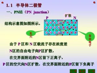
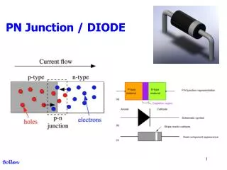
More positive than rest of N More negative than rest of P The PN Junction Diode Start with a P and N type material. Note that there are excess negatives in the n-type and excess positives in the p-type Merge the two – some of the negatives migrate over to the p-type, filling in the holes. The yellow region is called the depletion zone.
Biasing the Junction Apply a voltage as indicated. The free charge carriers (negative charges in the N material and positive charges in the P material) are attracted to the ends of the crystal. No charge flows across the junction and the depletion zone grows. This is called reverse bias. Switch polarity. Now the negative charges are driven toward the junction in the N material and the positive charges also are driven toward the junction in the P material. The depletion zone shrinks and will disappear if the voltage exceeds a threshold. This is called forward bias.
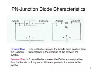
P material (anode) N material (cathode) Reverse Bias Forward Bias Diode Circuit Symbols
I-V Curve Recall Ohm’s Law (V=IR) Put it into slope-intercept form to get I = V/R. The slope of the graph is 1/R. Large slopes mean small R.
Types of Diodes • Rectifier Diode • Used in power supplies • Signal Diode • Used in switches, detectors, mixers, etc. • Zener Diode • Voltage regulation – operated reverse bias in the avalanche region • Reference Diode • Used like zener for voltage regulation
Types of Diodes • Varactor Diode • PN junction exhibits capacitive properties • Depletion zone acts like a dielectric • Adjacent material acts like the capacitor plates • Increasing reverse bias decreases capacitance – recall • Capacitance Effect is destroyed if the forward bias is great enough to destroy the depletion zone
Diode Tuning • Varactor used to tune a harmonic circuit, as before • Increasing reverse bias decreases C and increases fres
Rectification • Conversion of ac to dc. • Many devices (transistors) are unidirectional current devices • DC required for proper operation.
Bridge Rectifier Operation
Filters • We have now used diodes to produced a pulsed dc signal. • Most equipment requires “regulated” dc • We must remove the “ripple” • Ripple is departure of waveform from pure dc (flat, constant voltage level) • Frequency – so far we have seen pulsed dc at the same frequency as the input (½ wave) or twice the line frequency (full wave rectifier) • Amplitude – a measure of the effectiveness of the filter
Ripple Factor Low r indicates better filtering
Alternate Definition • Defined also for current • Iac = effective value of ac harmonic component • Idc = average of dc component For ½-wave rectifier r = 1.21 For full-wave rectifier r = 0.48
High Pass Filter • I is the same through both R and C When f is small, denominator is large and the voltage ratio is small. When f is large, denominator is almost one
Typical Results R = 0.1 MW C = 0.16 mF Why is it called a high pass filter?
Half Power Point • Note the point at which • This will make (Vo/Vi )2 = ½ • Recall that one form of power is V2/R, so the output power is half the input power at this frequency.
Low Pass Filter Low frequency means denominator is small and Vo / Vi 1 High frequency means denominator is large and Vo / Vi is small
Low Pass Results Note the half power frequency again.
Half Wave Capacitive Filter • Improving the ripple factor • During forward bias half-cycle, capacitor is charging • During the reverse bias half-cycle, the capacitor discharges through the output resistor
Full Wave Capacitive Filter • Even better ripple factor.
L-Section Filter Full wave rectifier, using ground loop on each half cycle • The series inductor opposes changes in current • The coil stores energy when the current is above average and • releases energy to the circuit when the current falls below average • Coil chops off (chokes) the peaks of the ac pulses • L-section delivers more steady current than the capacitive filter alone • Used for cases of variable loads where good regulation is required • Output voltage is less than the capacitive filter
P Filter Full wave rectifier, using ground loop on each half cycle Combines the effects of a capacitive and L-section filter. Regulation is poor when load varies, however.
Precise Voltage Regulation • If the load current is varying, but you require voltage to be constant, R must vary (V=IR).
The Avalanche Region • Increasing reverse bias on the diode eventually accelerates electrons in the depletion zone so that they ionize other atoms. • The freed electrons ionize other atoms • Avalanche occurs • Zener Diodes are designed so that the transition potential is very steep
Zener I-V Curve For a large change of current, voltage remains at VZ Zener acts like an automatically varying resistor. Can be obtained with VZ from 2.4 – 200 V.
Zener Regulation Circuit Since the load is in parallel with the diode, the voltage drop across RL is always the same as across VR1 and is VZ = constant Zener voltage The input voltage V must be greater than VZ. Zener MUST be operated under load. If not, the zener is still delivering power (more than usual) and may melt. Recall that the zener can draw large currents all at the same voltage.
Voltage Multiplication R protects D from surges When D is conducting, C charges to Vpeak During reverse bias half cycle, C discharges through load at the peak voltage Vout = Vpeak = 2 Vrms