Download
1 / 73
1k likes | 1.69k Views
Molecular Electronics. Prophecies of the Future of Technology are Risky!! For Example :. “I think there is a world market for maybe five computers.” T.J. Watson, President & CEO, IBM Corp., 1941-1956.

E N D
Prophecies of the Future of Technology are Risky!!For Example: “I think there is a world market for maybe five computers.” T.J. Watson, President & CEO, IBM Corp., 1941-1956 “There is no reason anyone would want a computer in their home.” Ken Olson, co-Founder, Digital Equipment Corp. (DEC) “640K ought to be enough for everybody.” Bill Gates, co-Founder, Microsoft Corporation. One of the wealthiest men in the world. “There is not the slightest indication that nuclear energy will ever be obtainable.” Albert Einstein, Nobel Laureate & one of the greatest scientists who ever lived!
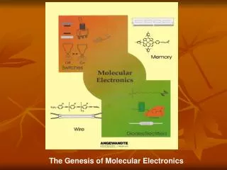
Molecular Electronics From Wikipedia: “Molecular Electronics(sometimes calledmoletronics)involves the study and application of molecular building blocks for the fabrication of electronic components. This includes both passive and active electronic components. Molecular electronics is a branch of nanotechology.”
Wikipedia Continued “An interdisciplinary field, molecular electronics spans physics, chemistry, & materials science. The unifying feature is the use of molecular building blocks for fabrication of electronic components. This includes passive (e.g. resistive wires) & active components such as transistors & molecular-scale switches. Due to the prospect of size reduction in electronics offered by molecular-level control of properties, molecular electronics has caused excitement in both science fiction & science. Molecular electronics provides a means to extend “Moore's Law”beyond the limits of small-scale conventional silicon integrated circuits. Molecular electronics is split into two related but separate subdisciplines: 1.Molecular materials for electronicsutilizes the properties of the molecules to affect the bulk properties of a material. 2.Molecular scale electronicsfocuses on single-molecule applications.
Source: Quantum Computing. 2004. A Short Course from Theory to Experiment. Joachim Stoltze and Dieter Stuter.
Moore’s “Law” • The number of transistors that can be fabricated on a silicon integrated circuit--and therefore the computing speed of such a circuit--is doubling every 18 to 24 months. • After four decades, solid-state microelectronics has advanced to the point at which 100 million transistors, with feature size measuring 180 nm can be put onto a few square centimeters of silicon
Silicon and Moore’s Law • Heat dissipation. • At present, a state-of-the-art 500 MHz microprocessor with 10 million transistors emits almost 100 watts--more heat than a stove-top cooking surface. • Leakage from one device to another. • The band structure in silicon provides a wide range of allowable electron energies. Some electrons can gain sufficient energy to hop from one device to another, especially when they are closely packed. • Capacitive coupling between components. • Fabrication methods (Photolithography). • Device size is limited by diffraction to about one half the wavelength of the light used in the lithographic process. • ‘Silicon Wall.’ • At 50 nm and smaller it is not possible to dope silicon uniformly. (This is the end of the line for bulk behavior.)
Moore’s “Second Law" X 1000$ generation Plant cost Mask cost
Moore’s second law. • Continued exponential decrease in silicon device size is achieved by exponential increase in financial investment. $200 billion for a fabrication facility by 2015. • Transistor densities achievable under the present and foreseeable silicon format are not sufficient to allow microprocessors to do the things imagined for them.
Electronics Development Strategies • Top-Down. • Continued reduction in size of bulk semiconductor devices. • Bottom-up (Molecular Scale Electronics). • Design of molecules with specific electronic function. • Design of molecules for self assembly into supramolecular structures with specific electronic function. • Connecting molecules to the macroscopic world.
Bottom-Up (Why Molecules?) • Molecules are small. • With transistor size at 180 nm on a side, molecules are some 30,000 times smaller. • Electrons are confined in molecules. • Whereas electrons moving in silicon have many possible energies that will facilitate jumping from device to device, electron energies in molecules and atoms are quantized - there is a discrete number of allowable energies. • Molecules have extended pi systems. • Provides thermodynamically favorable electron conduit - molecules act as wires. • Molecules are flexible. • pi conjugation and therefore conduction can be switched on and off by changing molecular conformation providing potential control over electron flow. • Molecules are identical. • Can be fabricated defect-free in enormous numbers. • Some molecules can self-assemble. • Can create large arrays of identical devices.
Molecules as Electronic Devices: Historical Perspective • 1950’s: Inorganic Semiconductors • To make p-doped material, one dopes Group IV (14) elements (Silicon, Germanium) with electron-poor Group III elements (Aluminum, Gallium, Indium) • To make n-doped material, one uses electron-rich dopants such as the Group V elements nitrogen, phosphorus, arsenic.
Molecules as Electronic Devices: Historical Perspective • 1960’s: Organic Equivalents. • Inorganic semiconductors have their organic molecular counterparts. Molecules can be designed so as to be electron-rich donors (D) or electron-poor acceptors (A). • Joining micron-thick films of D and A yields an organic rectifier (unidirectional current) that is equivalent to an inorganic pn rectifier. • Organic charge-transfer crystals and conducting polymers yielded organic equivalents of a variety of inorganic electronic systems: semiconductors, metals, superconductors, batteries, etc. • BUT: they weren’t as good as the inorganic standards. • more expensive • less efficient
Molecules as Electronic Devices: Historical Perspective • 1970’s: Single Molecule Devices? • In the 1970’s organic synthetic techniques start to grow up prompting the idea that device function can be combined into a single molecule. • Aviram and Ratner suggest a molecular scale rectifier. (Chem. Phys. Lett. 1974) • But, no consideration as to how this molecule would be incorporated into a circuit or device.
Molecules as Electronic Devices: Historical Perspective • 1980’s • Single Molecule Detection. • How to image at the molecular level. • How to manipulate at the molecular level. • Scanning Probe Microsopy. • STM (IBM Switzerland, 1984) • AFM
Molecules as Electronic Devices: Historical Perspective • 1990’s: Single Molecule Devices. • New imaging and manipulation techniques • Advanced synthetic and characterization techniques • Advances in Self-Assembly »» Macroscopic/Supramolecular Chemistry • These developments have finally allowed scientists to address the question: • “How can molecules be synthesized and assembled into structures that function in the same way as solid state silicon electronic devices and how can these structures be integrated with the macroscopic regime?”
Molecular Junction Mechanically-Controlled Break Junction Resistance is a few megohms. (Schottky Barrier)
Resonant Tunneling Diode Alkyl Tunnel Barriers Conduction between the two ends of the molecule depends on pi orbital overlap which in turn relies on a planar arrangement of the phenyl rings.
Negative Differential Resistance mNDR = molecular Negative Differential Resistance Measured using a conducting AFM tip One electron reduction provides a charge carrier. A second reduction blocks conduction. Therefore, conduction occurs only between the two reduction potentials.
Voltage-Driven Conductivity Switch Applied perpendicular field favors zwitterionic structure which is planar Better pi overlap, better conductivity.
Dynamic Random Access Memory Voltage pulse yields high conductivity State - data bit stored Bit is read as high in low voltage region
Voltage-Driven Conductivity Switch Device is fabricated by sandwiching a layer of catenane between an polycrystalline layer of n-doped silicon electrode and a metal electrode. The switch is opened at +2 V, closed at -2 V and read at 0.1 V.
Voltage-Driven Conductivity Switch High/Low Conductivity Switching Devices Respond to I/V Changes
Voltage-Driven Conductivity Switch n-type
Carbon Nanotubes Gentle contact needed Nanotube conductivity is quantized. Nanotubes found to conduct current ballistically and do not dissipate heat. Nanotubes are typically 15 nanometers wide and 4 micrometers long.
Molecular Self-Assembly • Self-Assembly on Metals • (e.g., organo-sulfur compounds on gold) • Assembly Langmuir-Blodgett Films • Requires amphiphilic groups for assembly • Carbon Nanotubes • Controlling structure
Cyclic Peptide Nanotubes as Scaffolds for Conducting Devices Hydrogen-bonding interactions promote stacking of cyclic peptides Pi-systems stack face-to-face to allow conduction along the length of the tube Cooper and McGimpsey - to be submitted CYCLIC BIOSYSTEMS
Spontaneous self-directed chemical growth allowing parallel fabrication of identical complex functional structures.
Nanopore Scanning Probe STM Break Junction Cross-wire Cui et al. Science 294 (2001) 571 Wang et al. PRB 68 (2003) 035416 Kushmerick et al. PRL 89 (2002) 086802 B. Xu & N. J. Tao Science (2003) 301, 1221 Electromigration H. S. J. van der Zant et al. Faraday Discuss. (2006) 131, 347 Molecular Electronics:Measuring single molecule conduction Nanocluster Mechanical Break Junction Dadosh et al. Nature 436 (2005) 677 Reichert et al. PRL 88 176804
Single-Molecule Conductivity L ELECTRODE R ELECTRODE MOLECULE
L ELECTRODE R ELECTRODE MOLECULE Molecular Orbitals Fermi energy
L ELECTRODE R ELECTRODE MOLECULE Molecular Orbitals eV V I
Finding a true molecular signature:Inelastic Electron Tunnelling Spectroscopy (IETS) I h/e V Elastic h/e V dI/dV Inelastic h/e V d2I/dV2 h/e V
Cui et al (Lindsay), Science 294, 571 (2001) “The resistance of a single octanedithiol molecule was 900 50 megaohms, based on measurements on more than 1000 single molecules. In contrast, nonbonded contacts to octanethiol monolayers were at least four orders of magnitude more resistive, less reproducible, and had a different voltage dependence, demonstrating that the measurement of intrinsic molecular properties requires chemically bonded contacts”.
6 5 4 I / arb. units 3 2 1 0 -1 -1 -0.5 0 0.5 1 I Ratner and Troisi, 2004 0.5 0.0 - 0.5 V (V)
Dynamics of current voltage switching response of single bipyridyl-dinitro oligophenylene ethynylene dithiol (BPDN-DT) molecules between gold contacts. In A and B the voltage is changed relatively slowly and bistability give rise to telegraphic switching noise. When voltage changes more rapidly (C) bistability is manifested by hysteretic behavior Lortscher et al (Riel), Small, 2, 973 (2006)
Switching with light Chem. Commun., 2006, 3597 - 3599, DOI: 10.1039/b609119a Uni- and bi-directional light-induced switching of diarylethenes on gold nanoparticles Tibor Kudernac, Sense Jan van der Molen, Bart J. van Wees and Ben L. Feringa “In conclusion, photochromic behavior of diarylethenes directly linked to gold nanoparticles via an aromatic spacer has been investigated. Depending on the spacer, uni- (3) or bidirectionality (1,2) has been observed.”
Nanotechnology 16 (2005) 695–702 Switching of a photochromic molecule on gold electrodes: single-molecule measurements J. He, F. Chen, P. Liddell, J. Andr´easson, S D Straight, D. Gust, T. A. Moore, A. L. Moore, J. Li, O. F Sankeyand S. M. Lindsay Current–voltage data (open circles) for (a) open molecules 1o and (b) closed molecules 1c
Temperature and chain length dependence Giese et al, 2002 Michel-Beyerle et al Xue and Ratner 2003 Selzer et al 2004
Conjugated vs. Saturated Molecules: Importance of Contact Bonding Au// S/Au Au/S S/Au Kushmerick et al., PRL (2002) negative bias Positive bias Au/S(CH2)8SAu 2- vs. 1-side Au-S bonded conjugated system gives at most 1 order of magnitude current increase compared to 3 orders for C10 alkanes! Au//CH3(CH2)7S/Au
Where does the potential bias falls, and how? Excess electron density Xue, Ratner (2003) Potential profile Galperin et al JCP 2003 • Image effect • Electron-electron interaction (on the Hartree level) Vacuum Galperin et al 2003